0
\$\begingroup\$

I came across this circuit and can't see how it works. I have never really dealt with any operation amplifier circuits that make use of positive feedback, so that only worsens the problem.
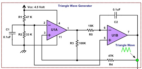
enter image description here

It seems that we have R1 and R2 forming a voltage divider for the input of U1A (about 1.9V). I have no idea what C1 is doing there since we are dealing with DC and the op-amp is high input impedance and to my knowledge does not do very much internal switching (thereby demanding current spikes). If C1 were in place to filter the supply then it's in an awfully strange place.

The second op-amp, U1B looks to be like some form of an integrator.

Any intuition into this circuit? How could you analytically go about solving this problem?

\$\endgroup\$
1
  • \$\begingroup\$ Here is someone else's schematic for a similar circuit in Circuitlab: circuitlab.com/circuit/gzdp75/triangle-generator-2, you can play around with probing different parts to see how it works. Also, note that you can remove C1 (C2 in their schematic) and the simulation will still work, but the purpose is to stabilize the voltage reference. \$\endgroup\$
    – Zuofu
    Commented Jun 15, 2014 at 23:06

2 Answers 2

5
\$\begingroup\$

You break it down into its different phases of operation. Yes, C1 is a filter capacitor; it's just there to make sure that the "reference" voltage going to the inverting input of U1A and the noninverting input of U1B is as noise-free as possible.

Yes, U1B is an integrator. It is simply integrating the output of U1A — which in turn must be a square wave, switching between two states.

U1A is functioning as a comparator. Its output is high when the noninverting input is higher than the reference voltage. Since the integrator has a negative coefficient, its output ramps down during this time.

Note that the feedback to U1A is a combination of the integrator output and its own output. This means that when the integrator ramps down low enough, the noninverting input of will eventually fall below the reference voltage, causing U1A to switch low. This positive feedback will immediately drive its own noninverting input more negative. Although the integrator output now starts moving in the positive direction, it now has some distance to go before it hits the U1A's switching threshold again.

This cycle simply repeats over and over.

\$\endgroup\$
4
\$\begingroup\$

That's a pretty much standard way of generating a triangular wave.

R1, R2, C1 provide a stable voltage reference. As you sense C1 is there to stabilize it in some ways, it's there to suppress noise, and that's not a strange place at all. The reference voltage is 1.85V

U1A, together with R3 and R4 is wired as a comparator, its input being the green node, while U1B, R5 and C2 are integrators.

I am assuming you know how to analyze circuits so I'm going to be quick, feel free to ask for clarifications.

Assuming that the op amps are rail to rail the voltage on the output of U1A is either Vcc or ground. Let's suppose that C2 is discharged, so V7=V6=V5=Vref=1.85V, and that V1=Vcc, then C2 starts to charge through R5 and V7 starts to fall. Since V1 is fixed if V7 falls then V3 falls, at some points it would go under Vref and V1 will go to ground. Now C2 starts to discharge through R5 and V7 rises, and so on.

The triangular wave angle is determined by C2 and by the current that flows in it, that depends on the value of R5 and Vref. The voltages at which the comparator switches are determined by Vref, R3 and R4. Selecting all these components you can then choose the frequency.

Please also note that since Vref does not equal Vcc/2 the triangular wave won't be triangular, i.e. one of its slopes will be steeper than the other.

\$\endgroup\$

Your Answer

By clicking “Post Your Answer”, you agree to our terms of service and acknowledge you have read our privacy policy.

Not the answer you're looking for? Browse other questions tagged or ask your own question.