3
\$\begingroup\$

I'm using Altium Designer 14.2.3 and I have a connector on which are always two pins connected to each other. In my schematic library I have configured the Pins to be hidden and connected to the other. (e.g Pin 7: hide [x] Connect To 6)

In the PCB I want to route to both pins for having a better connection, but altium doesn't let me do this.
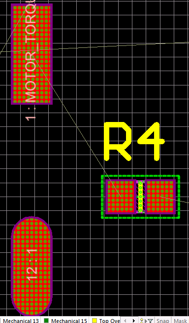
R4 should be connected to both pins

As shown in the image I want to connect R4 to pin 1 AND 12. Does anyone have a solution for this?

\$\endgroup\$

1 Answer 1

1
\$\begingroup\$

In "connect to" you should write the net name, not the pin number.

\$\endgroup\$
4
  • 1
    \$\begingroup\$ This would make sense. But I don't get how I could use a component from a library in different schematics when I have the pin connected to a defined net name. Do I have to use always the same net names when using this component? Should I use this method only for VCC and GND Pins? \$\endgroup\$
    – c0ff3m4kr
    Commented Jun 16, 2014 at 8:54
  • 1
    \$\begingroup\$ I found the solution. I leave the Pins connected to the Pin number in the library and in the schematic I edit the component in Properties > Edit Pins... > Edit to set the net label for each pin. Thanks for the answer! \$\endgroup\$
    – c0ff3m4kr
    Commented Jun 16, 2014 at 9:00
  • 1
    \$\begingroup\$ that's the reason i've given up to use this function in AD ))) \$\endgroup\$
    – Alexey
    Commented Jun 16, 2014 at 9:15
  • 1
    \$\begingroup\$ This issue is also explained here. \$\endgroup\$
    – gbmhunter
    Commented Oct 29, 2015 at 21:25

Your Answer

By clicking “Post Your Answer”, you agree to our terms of service and acknowledge you have read our privacy policy.

Not the answer you're looking for? Browse other questions tagged or ask your own question.