1
\$\begingroup\$

I read the data sheet of a shift register and I saw some tutorials on the internet. I can use all pins of my new shift register except pin 12. because I still don't understand what is the meaning of storage clock and how can I use it ? I use the clock of Pin 11 and I understand How a shift register works, only pin 12 is missing.

Datasheet :

http://elinux.org/images/2/2d/74hc595.pdf https://www.sparkfun.com/datasheets/IC/SN74HC595.pdf

Thanks in advance,

\$\endgroup\$

2 Answers 2

2
\$\begingroup\$

The storage register holds the data that is output from the 74HC595, and a rising edge on the ST_CP transfers the data currently in the shift register, into the storage register.

Without the storage register, the outputs would be driven directly from the shift register, and would therefore display the new data as it is being shifted into the chip. This could have undesirable results as the outputs would turn off or on unexpectedly.

With the storage register, the outputs don't change until you set ST_CP.

\$\endgroup\$
4
\$\begingroup\$

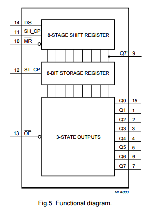
On page 5 of the first document a detailed block diagram is given: enter image description here

As you can see, in addition to the shift register, the part has also a storage register, that can be commanded to take the shift registers value and latch it. This command is given by ST_CP.

\$\endgroup\$

Your Answer

By clicking “Post Your Answer”, you agree to our terms of service and acknowledge you have read our privacy policy.

Not the answer you're looking for? Browse other questions tagged or ask your own question.