2
\$\begingroup\$

I preface this with saying that at one time, many many years ago, I had taken some EE courses. I remember only a little.

I was simulating a simple non-inverting amplifier used in a DC setting as a refresher and I noticed that depending on which model OpAmp I used, I got very different simulator results.

I was comparing the two datasheets and I don't see a significant difference.

                           LM324         LF412
Parameter                Min / Max     Min / Max
Input Offset Voltage     ?   / 3mV     ?   / 3mV
Input Bias Current       ?   / 100nA   ?   / 200pA
Input Offset Current         / 30nA       / 100pA
Input Common Voltage     0   / V+-1.5V -11V/ 11V
Supply Current           ?   / 1.2mA       / 6.5mA
Output Source Current    20mA/ ?       ?   / ?

The LM324 and LF412 data sheets. I am using this summary as a refresher as to what all these terms mean.

The parameter that I'm not certain about is Input Common-Mode Voltage Range.

I believe, because of the "virtual short circuit approximation", that both inputs (V+, V-) are at roughly the same voltage most of the time. So I don't think this affects the simulation, but I'm not sure.

All the other parameters appear to be within range of each other (or are in the pA/nA range so I'm ignoring them).

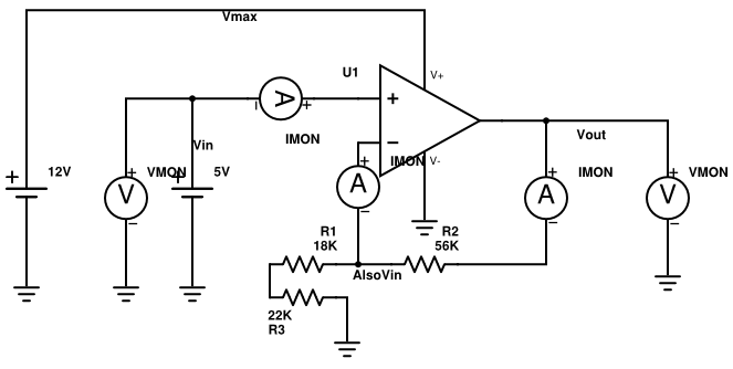
This is the circuit I'm testing. It's attempting to amplify the Vin voltage by 1.4 such that when Vin is in the range 0,5V DC then Vout is 1.4x higher in the range 0,12V DC (I'm aware that I will never reach 12V exactly).

Circuit

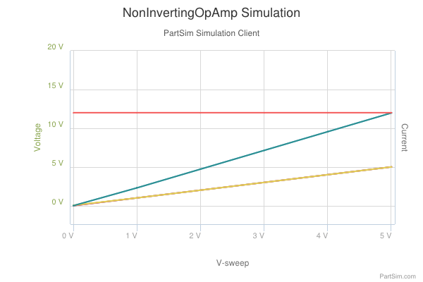
Here is the simulation using the LM324. This is the expected output:

LM312 Simulation

Vmax is orange

Vout is blue

Vin (the V+ input) is yellow

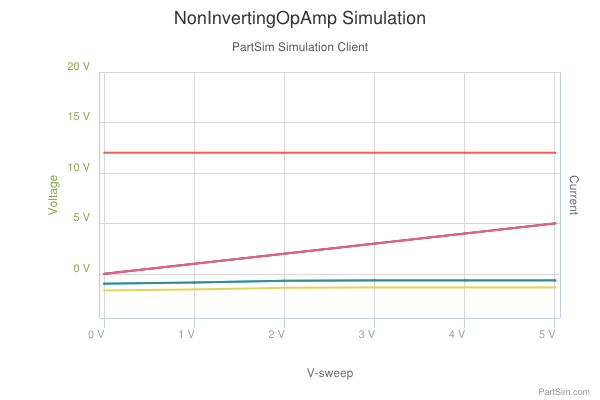
Here is the simulation using the LF412. This seems very wrong:

LF412 Simulation

Vmax is orange

Vout is blue

Vin (the V+ input) is purple

alsoVin (the V- input) is yellow

\$\endgroup\$
5
  • 2
    \$\begingroup\$ The input common mode range of LF412 is +/- 11 V, when the power supplies are +/- 15 V. If you use 0 V for the negative supply, it for sure won't work with an input common mode voltage below 4 V, and maybe won't work at all, since there's no specs for that situation. \$\endgroup\$
    – The Photon
    Commented Dec 3, 2015 at 6:35
  • 1
    \$\begingroup\$ See Fig 5 in the LF412 datasheet for "typical" common mode voltage effect from changing the negative supply voltage --- but still not including any prediction for what happens with 0 V supplied. \$\endgroup\$
    – The Photon
    Commented Dec 3, 2015 at 6:40
  • \$\begingroup\$ @ThePhoton I'm a bit confused about the LF412's datasheet for Input Common Mode Voltage Range. The Test Conditions cell is empty, but then every cell to the right is split. It almost looks like it is positive on top and negative on the bottom, except the top has some +/- as well. \$\endgroup\$
    – Huckle
    Commented Dec 3, 2015 at 7:48
  • \$\begingroup\$ @ThePhoton I guess Vs is just industry standard terminology or something? I don't see it defined in the data sheet anywhere. It does explicitly define V+ and V- as the positive and negative power supply inputs. I guess Vs=+/-11V is shorthand for V+=11V, V-=-11V? \$\endgroup\$
    – Huckle
    Commented Dec 3, 2015 at 7:55
  • \$\begingroup\$ No it's not. Vs is however the (balanced) supply voltage in the LF412 datasheet. The LM324 datasheet uses only V+ for that... and you'll notice they say that opamp (unlike LF412) is geared for single supply use. Now you know why. \$\endgroup\$ Commented Dec 3, 2015 at 12:45

2 Answers 2

6
\$\begingroup\$

Theory

schematic

simulate this circuit – Schematic created using CircuitLab

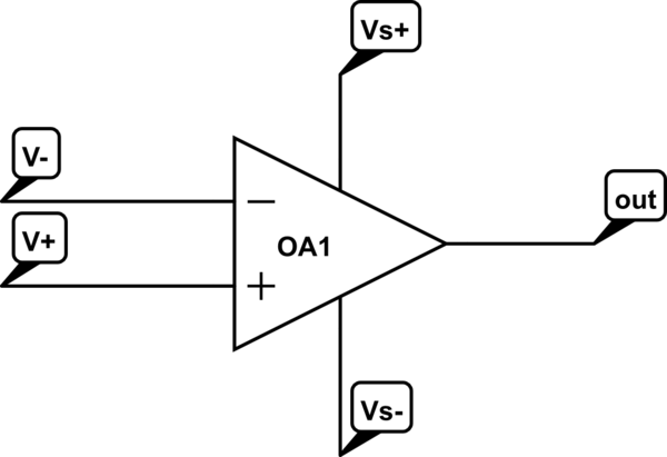
The input common mode voltage is a fancy way of saying the average voltage of the two inputs: \begin{gather} V_{cm} = \frac{V_{-} + V_{+}}{2} \end{gather}

When the op-amp is operated under negative feedback you may assume that \$V_{cm} = V_{-} = V_{+}\$.

The specification is there to tell you that there is some range of input voltages that you can expect the op-amp to function correctly. This is always within the supply given to the op-amp: \begin{gather} V_{s-}+A \le V_{cm} \le V_{s+}-B \end{gather} where \$A\$ and \$B\$ are non-negative numbers and properties of the op-amp. Of course, rather than giving you these two numbers directly they give a more useful quantity, which is the input common mode voltage range: \begin{gather} V_{cm-} \le V_{cm} \le V_{cm+} \end{gather} It is necessary for this condition to be satisfied if you want to expect the op-amp to function correctly.

Note that the parameters \$A\$ and \$B\$ are potentially non-linear functions of the supply voltage (and possibly other values such as output current). You have to check the datasheet to see how the common mode voltage range changes with supply voltage.

For example, take the LF412. In figures 4 and 5 it shows the common mode voltage as a function of positive and negative supply voltages (referenced against the average supply voltage). However, it simply is not specified below \$V_{s+} - V_{s-} \le 10V\$ because presumably the op-amp simply won't work correctly with less voltage.

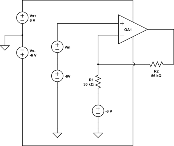
Now let's re-draw the circuit and pick a new ground point such that you get a symmetric supply:

schematic

simulate this circuit

In your graph, you are picking \$V_{in} \in [0V, 5V]\$. This corresponds to \$V_{+} \in [-6V, -1V]\$. Looking at figure 5 of the LF412's datasheet, the minimum common mode voltage allowed for a -6V negative supply is about -2.9V, or in the unshifted reference you're using of 3.1V.

TL;DR: PartSim's LF412 model is broken

This aside, for whatever reason Partsim's model for the LF412 is broken (most likely the pins are out of order). Luckily, you can get the model file here. Note that it needs a bit of tweaking to get it to work with partsim.

Here's the modified model:

*//////////////////////////////////////////////////////////
*LF412 LOW OFFSET, LOW DRIFT DUAL JFET INPUT OP-AMP MODEL
*//////////////////////////////////////////////////////////
*
* connections:  non-inverting input
*               |   inverting input
*               |   |   positive power supply
*               |   |   |   negative power supply
*               |   |   |   |   output
*               |   |   |   |   |
*               |   |   |   |   |
.SUBCKT LF412N  1   2  99  50  28
*
*Features:
*Fast settling time (.01%) =           2uS
*High bandwidth =                     3MHz
*High slew rate =                   10V/uS
*Low offset voltage =                  1mV
*Low supply current =                1.8mA
*NOTE: Model is for single device only and simulated
*      supply current is 1/2 of total device current.
*
IOS 2 1 25.0P
CI1 1 0 3P
CI2 2 0 3P
R1 1 3 1E12
R2 3 2 1E12
I1 99 4 1.0M
J1 5 2 4 JX
J2 6 7 4 JX
R3 5 50 650
R4 6 50 650
*Fp2=28 MHZ
C4 5 6 4.372P
I2 99 50 800UA
EOS 7 1 POLY(1) 16 49 1E-3 1
R8 99 49 80K
R9 49 50 80K
V2 99 8 2.13
D1 9 8 DX
D2 10 9 DX
V3 10 50 2.13
EH 99 98 99 49 1
G1 98 9 5 6 20E-3
R5 98 9 10MEG
VA3 9 11 0
*Fp1=18 HZ
C3 98 11 857.516P
*Fp=30 MHz
G3 98 15 9 49 1E-6
R12 98 15 1MEG
C5 98 15 5.305E-15
G4 98 16 3 49 1E-8
L2 98 17 144.7M
R13 17 16 1K
F6  99 50 VA7 1
F5  99 23 VA8 1
D5  21 23 DX
VA7 99 21 0
D6  23 99 DX
E1  99 26 99 15 1
VA8 26 27 0
R16 27 28 50
V5  28 25 0.646V
D4  25 15 DX
V4  24 28 0.646V
D3  15 24 DX
.MODEL DX D(IS=1E-15)
.MODEL JX PJF(BETA=1.183E-3 VTO=-.65 IS=50E-12)
.ENDS
*$

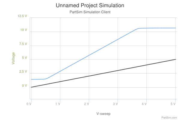
Here's the simulation results with the fixed model (\$V_{out}\$ is blue, \$V_{+}\$ is black):

enter image description here

Interestingly the output doesn't quite line up with theory; that's because I simply assumed that because figure 5 of the datasheet doesn't show the negative supply voltage vs. common mode voltage range it won't work below that. Instead, it is simply unspecified. The model just happens to work below that, though I don't know which behavior you'll actually get in real life.

\$\endgroup\$
3
  • \$\begingroup\$ The LM324 model is broken, too. There's no way the output will go smoothly from 0 to 12V. They must be using some kind of ideal op-amp model here, not anything like a real op-amp. \$\endgroup\$ Commented Dec 3, 2015 at 8:26
  • \$\begingroup\$ True, I didn't notice that before. Luckily, TI also has spice models for the LM324. \$\endgroup\$ Commented Dec 3, 2015 at 8:42
  • \$\begingroup\$ Also, apparently I can't do math because 18+22 != 30 :P I think this is an appropriate excuse \$\endgroup\$ Commented Dec 3, 2015 at 18:22
3
\$\begingroup\$

The standard Boyle opamp macromodel that is used for most old opamps does not model the common mode input range.

However, temperature performance, common-mode input range, offset voltage, offset current, input protection, power supply rejection, noise, THD, input impedance, good ac output resistance, and change in supply current versus supply voltage are a few of the more important parameters that are not modelled with the Boyle macro topology.

Currently TI only gives a basic Boyle model for LM324 (and gives nothing for LM324-N). Things get more interesting for LF412. For the bog standard one, you also get only a Boyle model indetified as "LF412C" inside the file. But for LF412-N you do get a model (identified as "LF412/NS" inside the file) that has common-mode effects. Downloader beware.

Of course I have no idea what partsim uses. The saying "show me the code" translates into "show me the model" when it comes to opamp SPICE simulations beyond the very basics.

Now to more practical matters. First you say:

It's attempting to amplify the Vin voltage by 1.4 such that when Vin is in the range 0,5V DC then Vout is 1.4x higher in the range 0,12V DC (I'm aware that I will never reach 12V exactly).

That's not how it's gonna work, because of the non-inverting configuration, the factor is going to be 2.4 (1+Rf/Rg).

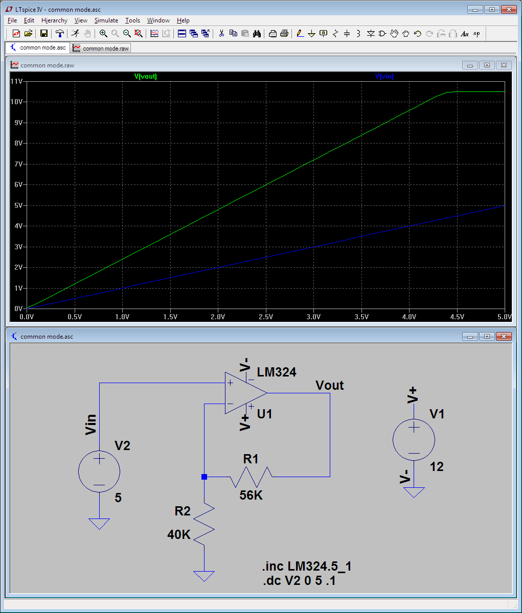
But leaving that aside, even with TI's LM324 model you at least get it to limit output below the 12V rail... which is more than partsim manages:

enter image description here

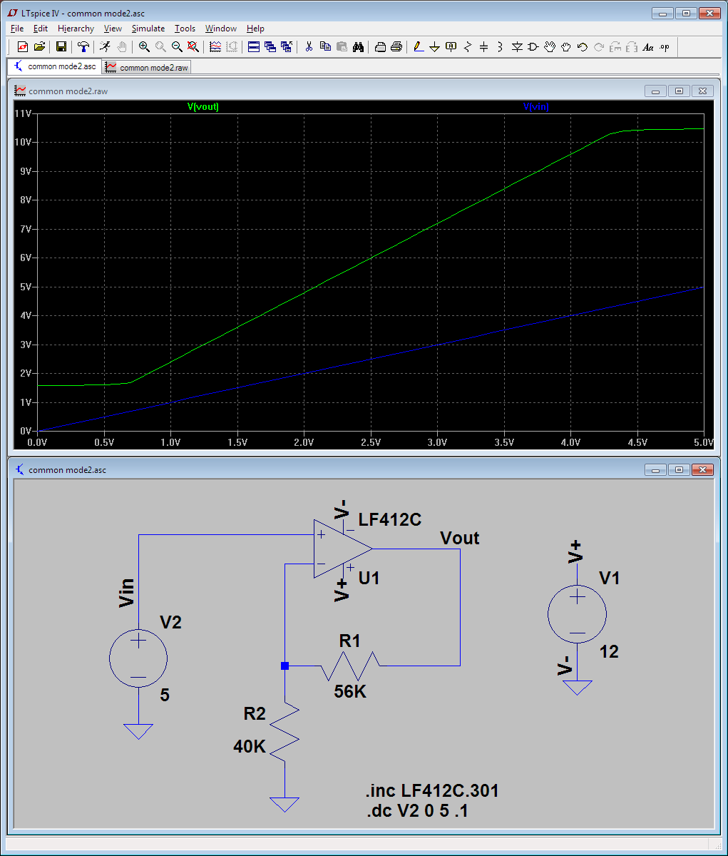
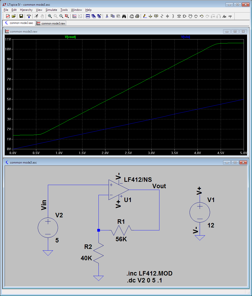
Here's the LF412C, this can't swing all the way down to 0:

enter image description here

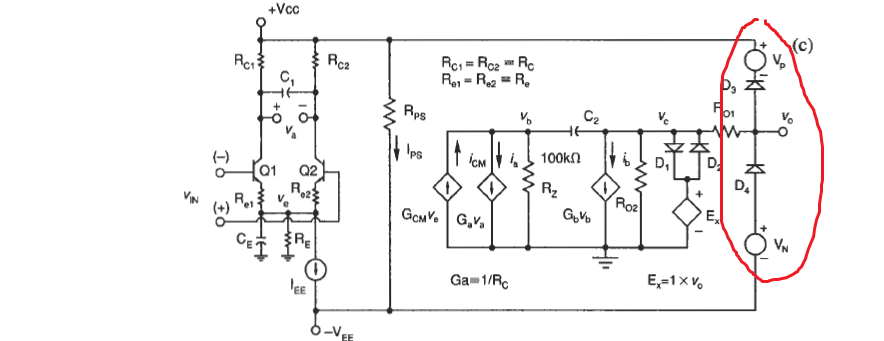
And here's how it works; you'll want to refer to the Boyle schematic while reading the stuff below. I've circled the parts that simulate the rail-related limits for the output.

enter image description here

For LM324, the voltage sources in series with the diodes (that simulate the rail limits, this is the right-most are set to

DC    5 53 DX
DE   54  5 DX
VC    3 53 DC 2.100
VE   54  4 DC .6

So on the low side it goes to 0 after the diode drop is subtracted, but the high side goes to about 10.5V (2.1-diode drop).

For the LF412C now we have

VC    3 53 DC 2.200
VE   54  4 DC 2.200

So both sides (high an low) limited to about 1.6V from the rail. This is how they simulate that LM324 is capable of single supply operation, but LF412 isn't.

I have to see now what the fancier LF412NS model buys here, if anything. Well, no real difference

*********OUTPUT VOLTAGE LIMITING********
V2 99 8 2.13
D1 9 8 DX
D2 10 9 DX
V3 10 50 2.13

enter image description here

I have to yet grok what parts of the code/deck about common-mode in that latter model actually do, but it doesn't seem to add any obvious input range limitations besides what the output swing limitations already impose (as a result).


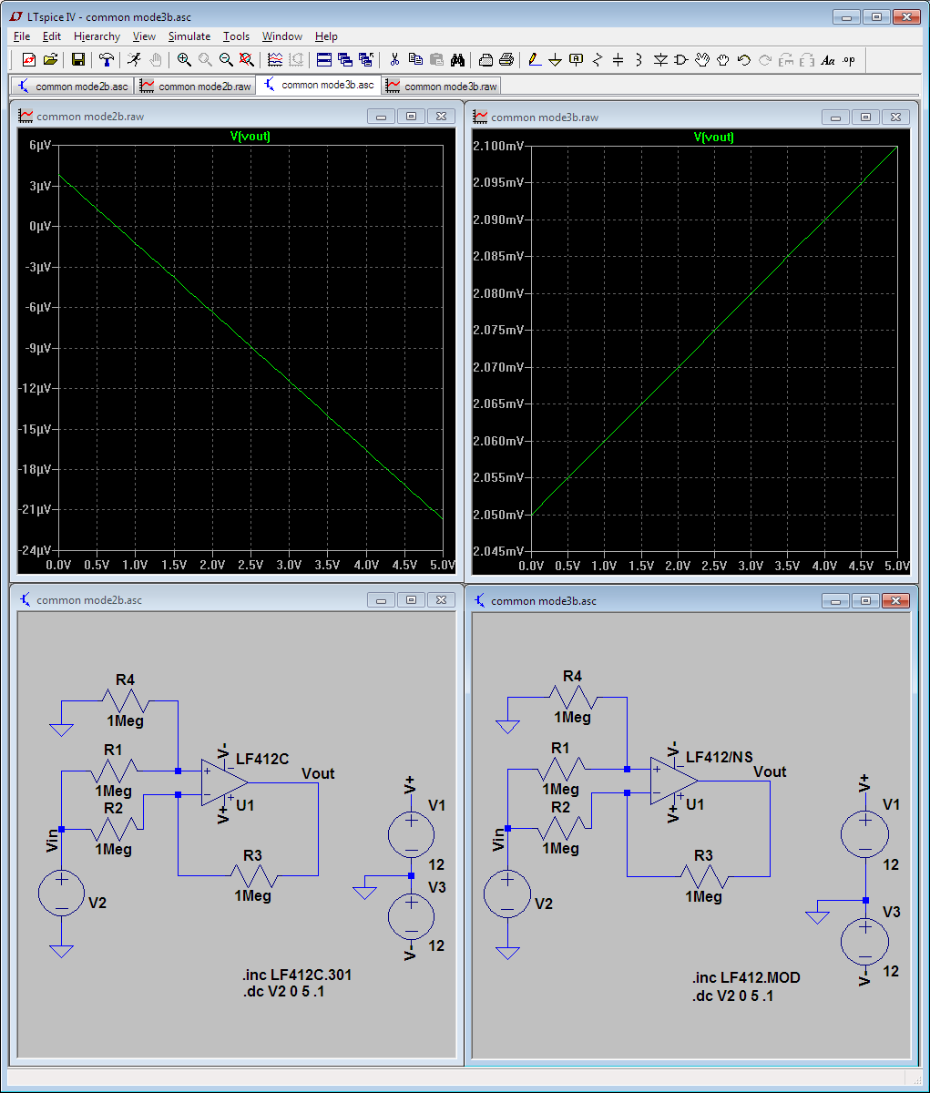
I think I figured out what the addition is in the NS model. LF412 (incl. N variant) datasheet has a typical CMRR of 100dB. That means for a 5V common mode voltage a change in the output of 50uV. With the 412NS model we get exactly that "common mode effect". With the 412C model it's some seemingly random stuff/value.

enter image description here

There is however not simulation of the common-mode input range in the latter either, it seems.

\$\endgroup\$
3
  • \$\begingroup\$ Given that the PartSim model is pretending the LM324 is fully rail-to-rail, are they even using this Boyle model? From the plots above, it looks like an ideal op-amp model, not anything trying to model reality. \$\endgroup\$ Commented Dec 3, 2015 at 13:54
  • \$\begingroup\$ @WarrenYoung: Indeed I just simulated in LTspice that, I get rail limitation with TI's 324 model. Stay tuned for some updates. \$\endgroup\$ Commented Dec 3, 2015 at 13:56
  • \$\begingroup\$ I mispoke. Obviously 5 * 2.4 = 12. My resistor ratio is 1.4 (as it should be). I am also well aware of the inability to get right to the power supply voltage (I stated that in the question). \$\endgroup\$
    – Huckle
    Commented Dec 3, 2015 at 17:49

Your Answer

By clicking “Post Your Answer”, you agree to our terms of service and acknowledge you have read our privacy policy.

Not the answer you're looking for? Browse other questions tagged or ask your own question.