15
\$\begingroup\$

enter image description here

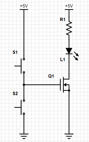
In the circuit above, when S1 is pressed and released, the LED turns ON and stays ON. Why is this so? I can't directly measure the Gate Voltage with a DMM since connecting the DMM results in the LED not staying ON.

If the LED is ON (S1 pressed then released), when S2 is pressed and released, the LED turns OFF, as expected.

I skimmed my intro ECE book chapter on FETs and it didn't seem to mention anything about this phenomenon...

\$\endgroup\$
6
  • 1
    \$\begingroup\$ If, when the LED is off and you connect your meter across S1 you should be able to turn the LED on. Even the very high resistance of the meter will pass enough current to charge and discharge the FET gate. \$\endgroup\$
    – Transistor
    Commented Jan 17, 2016 at 21:34
  • \$\begingroup\$ So will/should your fingers (welcome to skin resistance.) (the human kind, not the wire skin-depth kind) \$\endgroup\$
    – Ecnerwal
    Commented Jan 17, 2016 at 22:26
  • 7
    \$\begingroup\$ That switch setup is just asking for a dead short \$\endgroup\$
    – Passerby
    Commented Jan 17, 2016 at 22:38
  • \$\begingroup\$ Also, your Book probably does mention this by saying you need a pull-down resistor to fully shut the Fet off \$\endgroup\$
    – Passerby
    Commented Jan 17, 2016 at 22:46
  • \$\begingroup\$ Aside from the correct answers, explaining the role of the gate capacitance, you should never leave gates "floating" (not connected to some low impedance < 1 MOhm circuit); because of high impedance gate will pick up random noises or, in the worst case, the FET can get completely destroyed. \$\endgroup\$
    – ilkhd
    Commented Jan 18, 2016 at 9:34

2 Answers 2

24
\$\begingroup\$

When you press S1, you're storing a charge on the gate which has a small capacitance Cgs. This charge maintains the electric field which keeps the channel between the drain and source. Once you press S2, the charge on the gate is deplected and the channel is turned off

\$\endgroup\$
3
  • 2
    \$\begingroup\$ +1 It should be mentioned that the MOSFET will have a small amount of leakage (small, but probably many orders of magnitude lower than the numbers shown in the datasheet as maximums), so eventually the MOSFET will settle out at some level (on, off or somewhere inbetween) regardless of which switch was last pressed. It might take days to get close at room temperature. This is basically how dynamic (and EEPROM) memory cells work. \$\endgroup\$ Commented Jan 17, 2016 at 21:47
  • \$\begingroup\$ If you replace S2 with a 10K resistor then S1 will work as expected, because the resistor will discharge the gate-source capacitance when S1 is released. \$\endgroup\$
    – Steve G
    Commented Jan 17, 2016 at 21:52
  • 3
    \$\begingroup\$ @SteveG - you seem to be missing the point of fun FET tricks... \$\endgroup\$
    – Ecnerwal
    Commented Jan 17, 2016 at 22:03
9
\$\begingroup\$

The gate of a MOSFET has a very, very high DC resistance. For all intents and purposes, it basically doesn't consume any current at all if it's just sitting at some steady-state value (we're talking femto-amps or less).

Also, MOSFET gates all have 'parasitic capacitance', which is essentially a couple of little tiny capacitors (usually a few pF) that connect the gate to the drain and the source.

When you press switch S1, you let in a whole bunch of charge from the +5V rail, which turns on the MOSFET. The trick is that it also charges up the gate's parasitic capacitors. When you release S1, all that stored charge has nowhere to go. It doesn't get consumed by the MOSFET's gate (since the gate doesn't consume any current), and also doesn't have any path to get back to ground.

Since the charge has nowhere to go, it just sits there and maintains +5V on the gate until you connect something else (such as S2 or your multimeter) and provide a path for the charge the take back to ground.

edit: fun fact, this phenomenon is also exactly how NAND Flash works.

\$\endgroup\$
1
  • 3
    \$\begingroup\$ Just to be clear, there aren't 'parasitic capacitors' that are sort of additional extras to the MOSFET - the input capacitance of a MOSFET is a fundamental property of the device, because the gate electrode is separated from the drain-source channel by a thin layer of dielectric material. Also the input capacitance of a typical power MOSFET device can easily be a couple of nanofarads, not pF. \$\endgroup\$
    – nekomatic
    Commented Jan 18, 2016 at 9:59

Your Answer

By clicking “Post Your Answer”, you agree to our terms of service and acknowledge you have read our privacy policy.

Not the answer you're looking for? Browse other questions tagged or ask your own question.