I was researching here on transistor amplifiers:
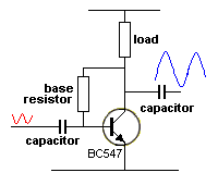
http://www.talkingelectronics.com/projects/TheTransistorAmplifier/TheTransistorAmplifier-P1.html#Stage and they were talking about these two transistor amplifiers. I use the one on the left because my circuits function better.
When I built my regen receiver, it utilized negative feedback in all stages and the circuit operated fine. If however, I took the class C approach, then the regen wouldn't oscillate as well.
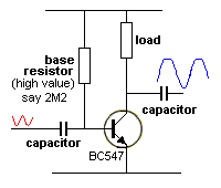
I then read on the site in regards to the circuit on the right:
This stage produces the maximum voltage amplification but it is very difficult to "set-up" because the value of the base resistor will either make the collector voltage nearly zero or full rail voltage. It is very difficult to get the collector to sit at mid rail. If the base resistor is a high value, the collector will sit at rail voltage. If the base resistor is a low value, the collector will sit a 0v. If a transistor with a different gain is fitted, the collector voltage will change completely. If it sits at mid-rail, the noise produced by the transistor will make the collector voltage rise and fall and produce a lot of noise.
In a transmitter, I want to be able to transmit the signal I want, not a bunch of random noise that a transistor produces.
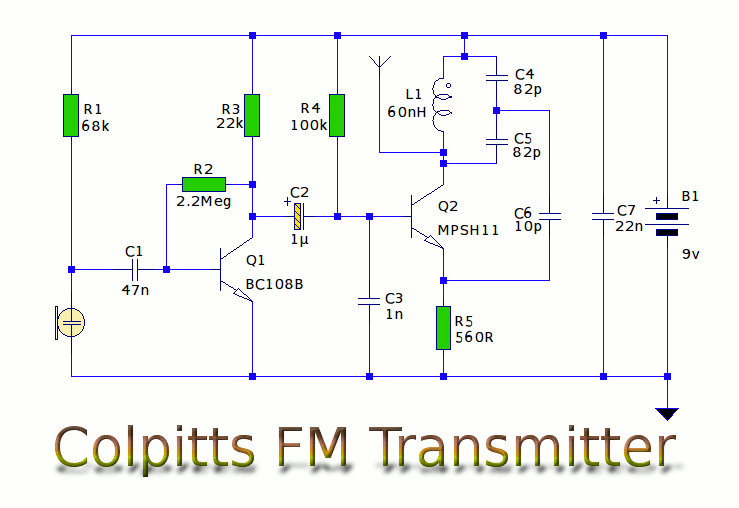
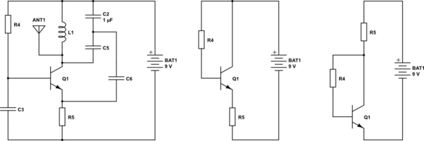
I then go find a random transmitter design from the internet and resistor R4 is connected from base to VCC instead of from base to collector of the same transistor. Why is that?


