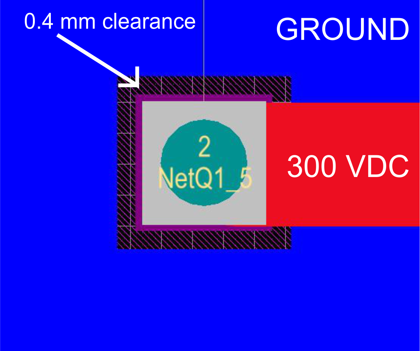
I'm designing a board that works with 300 VDC peak. I understand that there are rules for trace to trace PCB clearance. But what about Pin to ground pour clearance? I have not seen any standard specify this kind of clearance. This is one of the pin that I have on my PCB design. What should be the minimum pin-to- ground pour clearance to use?:
-
3\$\begingroup\$ GND pour is just a big fat version of a GND trace. \$\endgroup\$– PlasmaHHCommented Sep 21, 2016 at 9:35
-
2\$\begingroup\$ Yeah, why do you think trace to GND clearance should be any different from trace to trace clearance? High voltage won't care about trace names or geometry - if the clearance is too small it will arc through it. \$\endgroup\$– Dmitry GrigoryevCommented Sep 21, 2016 at 9:48
1 Answer
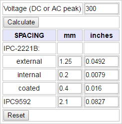
Clearance is clearance. It doesn't matter what type of conductors you're creating clearance for, whether they be pins/pads, traces, pours, etc. What's important, however, is that you make note of whether the connections are internal, external, or coated. For example, to find the required clearance for between two pins you have to use the number for external conductors, whereas if you have two traces on internal layers you can use the number for internal conductors. In your case you need to find the required clearance between an external conductor and a (presumably) coated conductor (it looks like your board is 2-layer, which means both the top and bottom layers will most likely be coated with soldermask). IPC-2221B states that for 300V DC you'll need a clearance for external conductors of 1.25mm, for internal conductors of 0.2mm, and for coated conductors of 0.4mm.
Since your ground pour is coated you should be able to use the 0.4mm figure (like you are showing). I generally try to give it a little extra space when I can, though. You seem to have plenty of room, so why not double the clearance, just to be safe?


