Guys I am new to the PCB design. The PCB I am designing has a connection to 4.5KV. I have a question related to the ground pour, should I avoid the ground pour on the entire top layer or should I just avoid the area around the 4.5KV connection (it’s an IGBT). In case avoiding only the IGBT area is sufficient how much should be the clearance. Moreover, it would be helpful to know what other problems can arise by having such high voltage on the PCB.
-
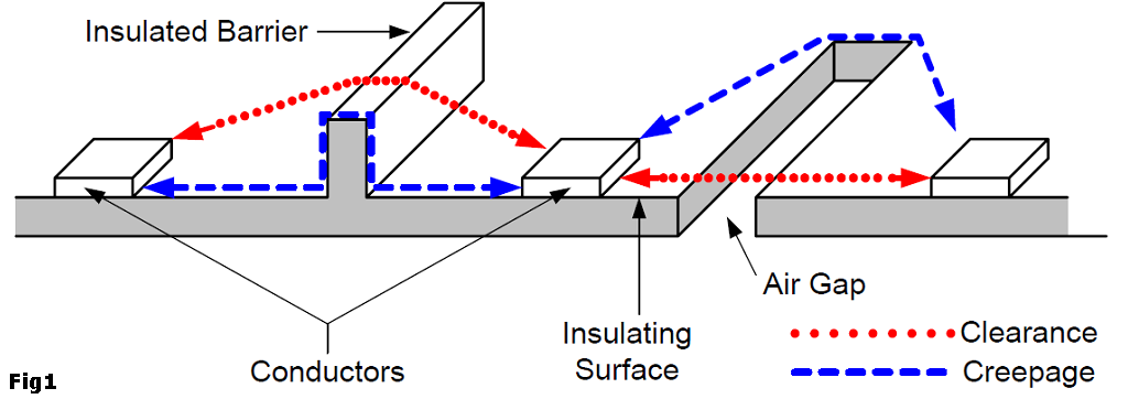
\$\begingroup\$ You require a minimum creepage distance with respect to the long-term RMS value. Depending on available PCB space you may require an air gap. Furthermore you need enough clearance to withstand expected maximum transient over voltages. Your question with respect to the GND pour is probably hard to answer without knowing details about your design. \$\endgroup\$– RevCommented Nov 28, 2018 at 12:49
2 Answers
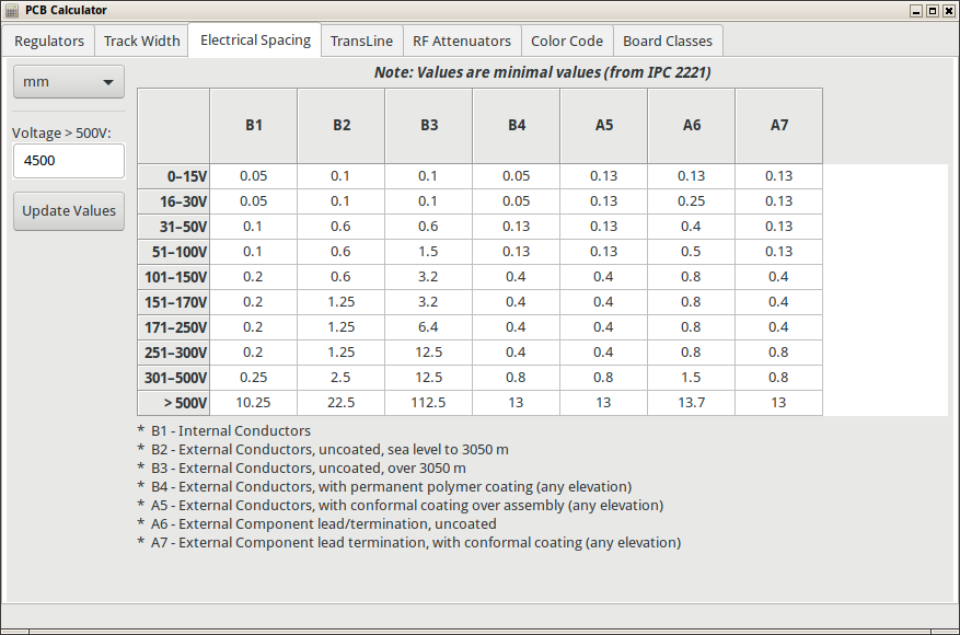
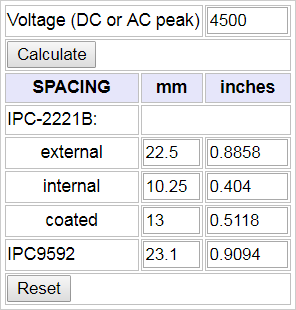
IPC-2221 specifies recommended clearance rules for given peak voltages. Based on this calculator, per IPC-2221B you need a minimum of 13 mm (512 mil) clearance between the high voltage traces and surrounding copper/components, assuming your traces are on the top or bottom layer and are coated with soldermask.
When working with such high voltages, it is advisable to include a creepage gap as well - a slot in the board between the high voltage section and the rest of the board to prevent any arcs from tracking along the surface.
This combined with the above clearance requirement should help protect your board from undesired arcing.
The IPC-2221 has already been stated as a source of information with regards to creepage.
 IPC-2221 tool from within KiCAD
However, this is only part of the story. The IPC-2221 rules are quite robust for internal or coated traces. However, they are overly pessimistic when it comes to uncoated traces, especially at altitude (Pachen's curve considerations) and equally do not fully take into consideration pollution levels.
The BE EN-60664 Insulation coordination for equipment within low-voltage systems is an additional specification to consider. While it only directly pertains to low voltage (50V -> 1000V), it does capture considerations with regards to partial discharge, the inception point as well as altitude and pollution.
As to other considerations.
Oblong pads. Besides benefits for lead-free and retention force, the lack of corners is extremely beneficial for higher voltage. Since charge concentrates around points you would want to minimise these wherever possible. This includes pads, copper fills and trace bends.
Multi-layer. You will probably want to take credit for FR4 with regards to voltage withstand and make use of the z-axis to realise routing. While FR4 has quite a strong dielectric strength and can easily support 4.5kV, poor FR4 cannot. If there is voids within the weave this presents a pocket of air not FR4 to the higher potential and there will be corona discharge within these voids until there is full breakdown. My advice is rely on x-y for creepage and IF you really need to use the z-axis, please specify a minimum of double pre-preg between laminates. Why two? the odds of two voids aligning is considerably lower than one void aligning with your potential


