1
\$\begingroup\$

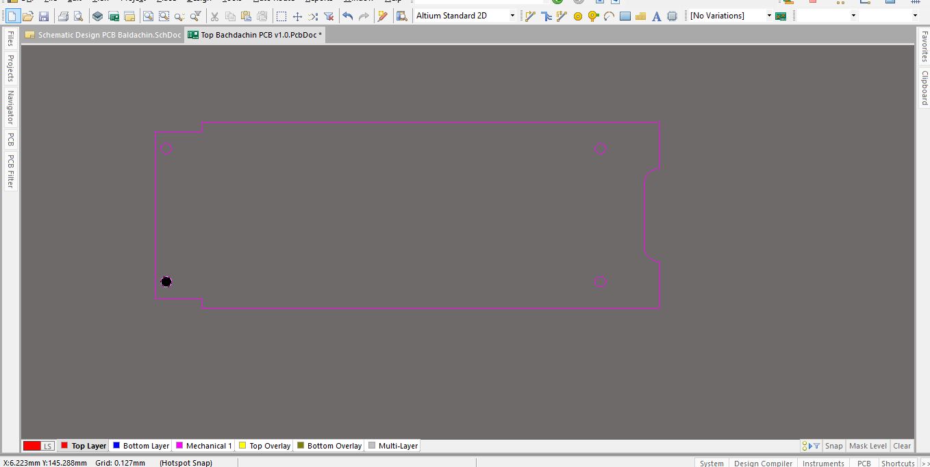
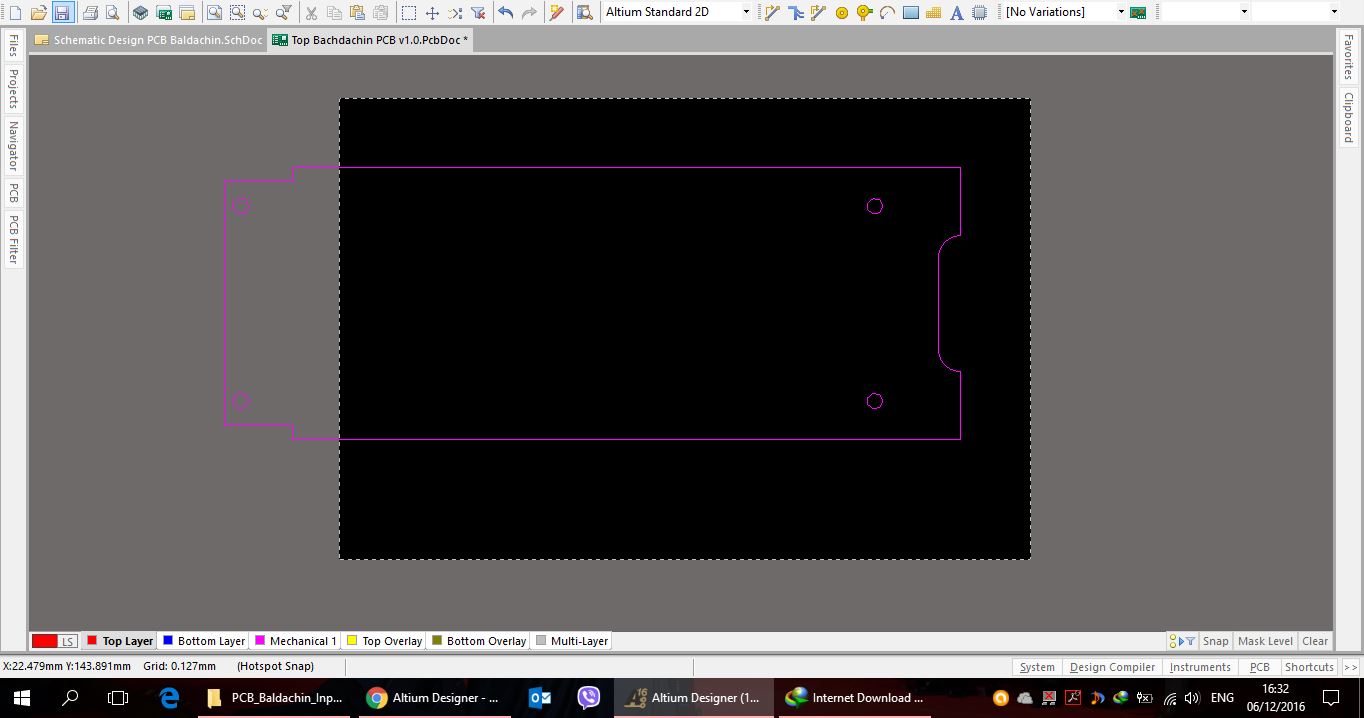
I have a shape for my PCB as follows in the picture below which includes four holes.

Desired Shape PCB on Altium

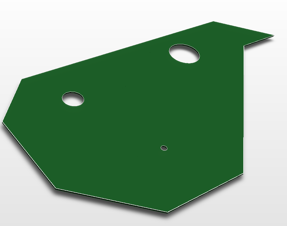
However, when I select the whole shape on Altium Designer and then select PCB from selected shape, it will only leave me the PCB as small round as you can see in this picture:

Image description

I wonder how can I make the PCB shape keeping the outer shape as the boarders of the PCB where the 4 circles are holes/vias.

\$\endgroup\$
3
  • \$\begingroup\$ Have you only selecting the outer shape? I guess the board shape algorithm isn't smart enough to detect shapes within shapes and just uses the first closed shape it "scans". \$\endgroup\$
    – Rev
    Commented Dec 7, 2016 at 9:05
  • \$\begingroup\$ I selected everything... How can I select only the outer shape? @Rev1.0 \$\endgroup\$ Commented Dec 7, 2016 at 9:11
  • \$\begingroup\$ It depends. Where does the shape come from? If it consists of loose primitives you should be able to select the respective lines by holding shift or control and left clicking/drag selecting. \$\endgroup\$
    – Rev
    Commented Dec 7, 2016 at 9:59

2 Answers 2

2
\$\begingroup\$

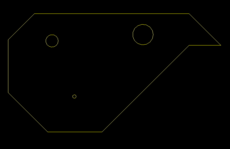
The above answer does not account for the holes, which was your question. I've shown below the correct answer on how to do this, creating a quick example PCB to illustrate.

enter image description here

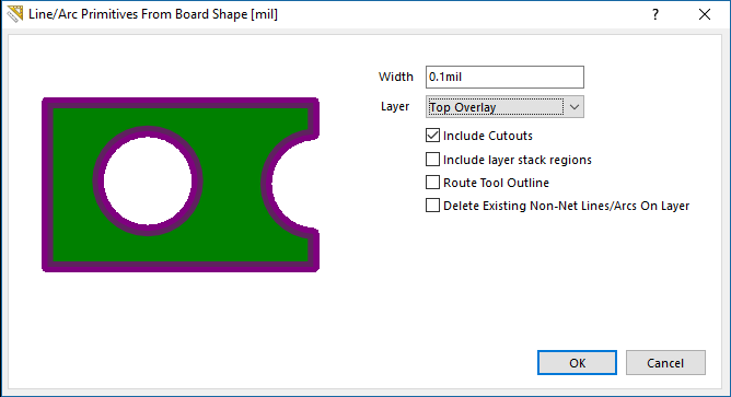
Select all shapes from your DFX file. Design -> Board Shape -> Define from Selected Objects. As you note, even selecting "cutouts" here doesn't do what you'd like. I think it's a bug.

enter image description here

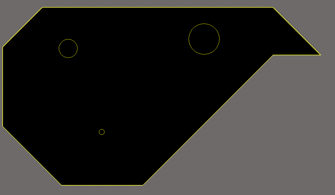
And the resulting board shape.

enter image description here

Now select the holes. For some reason I had to do this step for each one, it wouldn't let me batch select. Tools -> Convert -> Create Board Cutout from Selected Primitives.

The resulting PCB including holes:

enter image description here

If this answer solved your problem, please consider selecting it as the correct one. Thanks, and hope this helps.

\$\endgroup\$
1
\$\begingroup\$

First check if you have closed lines. Go to PCB inspector and check line connections. Select each of the line with Shift pressed (multi select), go to Design-> Board Shape ->Define from selected objects

Automatic algorithm is not good for that.

\$\endgroup\$
4
  • \$\begingroup\$ Yes dear @Rafal, it cannot detect that those are VIAs. I will see how it can be done manually. Any suggestions? \$\endgroup\$ Commented Dec 7, 2016 at 10:07
  • \$\begingroup\$ Which Altium do you have? @Joel Wington suggested answer, it works for me too. My answer also works for me with Altium 10 and 14. \$\endgroup\$
    – Rafal
    Commented Dec 7, 2016 at 20:21
  • \$\begingroup\$ @Rafal Interesting, it didn't work for me. I've got Altium 16 latest. \$\endgroup\$ Commented Dec 8, 2016 at 0:01
  • \$\begingroup\$ @JoelWigton maybe kind of bug or something. Unfortunately I do not have Altium 16 to try it out. \$\endgroup\$
    – Rafal
    Commented Dec 8, 2016 at 14:31

Your Answer

By clicking “Post Your Answer”, you agree to our terms of service and acknowledge you have read our privacy policy.

Not the answer you're looking for? Browse other questions tagged or ask your own question.