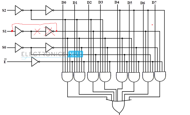
I'm reading a page on multiplexers that has the following image. I says for constructing one it used 7 not gate. But looking at the image I don't know why three of them are needed. Could't you just cut down on the number of them by making a connection such as what I've done in red bellow? Is there something else I'm missing here?
2 Answers
Yes, that could be removed and it would logically be correct, but there are a couple practical reasons why you wouldn't want to do that.
Those NOT gates are functioning as buffers for the signal coming in. This way, your single input signal doesn't need to drive a whole bunch of AND gate inputs. While this isn't a big deal for CMOS logic since input current is negligible (or at least very small) and doesn't affect the output voltage as much, TTL logic is more sensitive as it requires current to be drawn through the outputs. Three or four AND gates from one signal could be problematic as it will try to draw a lot of current. Even for CMOS inputs, which look close to a capacitor, the edge shapes of the incoming signals will be affected when they drive more gates (this is one reason why chips such as "clock buffers" exist and are very useful). Too many gates and suddenly your signal doesn't have enough time to finish driving every gate low before it starts to go high again (your waveform then starts to look like this and doesn't ever get all the way low or high) because it has to charge and discharge all those capacitors, making what effectively is an RC filter on your signal (R is the output impedance of your driver).
The other thing about using those as buffers is it makes the inputs all look the same electrically. Your ~E input drives 8 AND gates while the other inputs drive around 4. This means that you need to compensate for each individual input when interfacing to the circuit, rather than being able to use the same output circuit to drive the inputs. With those buffers, all of the pins, including the D pins, look the same as any other pin and make designing with this logic block easier to do.
I think it all comes down to "it makes it easier to design to use this particular circuit."
-
\$\begingroup\$ Huh. Interesting. Thanks a lot for the in depth answer! :) \$\endgroup\$– windy401Commented Feb 23, 2017 at 4:49
In terms of the truth table, you are correct. If you made the change you indicate, the logical function would be identical.
Most likely the reason for it is that the first NOT gate is acting as a signal buffer to provide fanout. If you made the connection you have indicated, the then input line S1 (presumably coming from a PCB) would have to drive 9 gates in parallel. Depending on the logic family and speed, there will be some maximum fanout ratio. Even if the application supports a fanout of >9, it is common to run several multiplexers sharing the same control lines to mux a multi-bit signal. By adding a second NOT gate to each input, you only have to drive a single gate and the fanout happens on chip.

