1
\$\begingroup\$

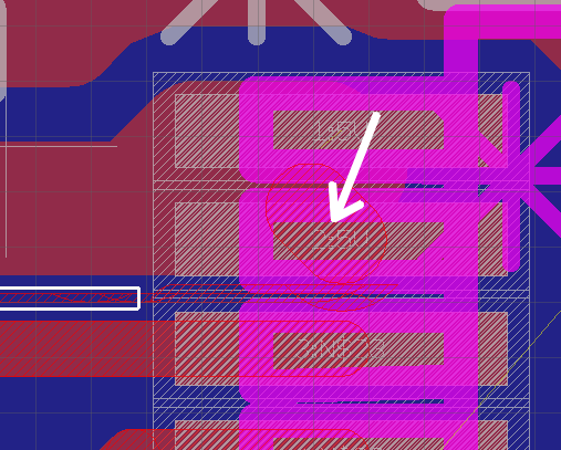
Designing a PCB in Eagle, and I have mysterious areas that throw 'clearance' and 'width' errors. I don't know where they come from, and I have been unable to move, or click on them to see why they are present. Has anybody seen this problem before, or know what may be causing it?

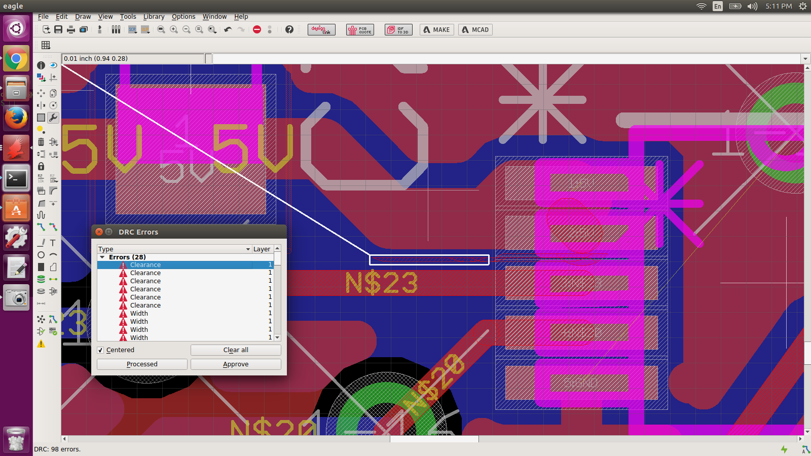
The image shows an example area that is throwing an error. The areas are in the 'top layer', but are shown as red hashed surfaces, as opposed to solid.

enter image description here

\$\endgroup\$
2
  • 2
    \$\begingroup\$ Those are standard clearance and width errors. The distance between the tracks (5V and N$23) is less than your clearance rules allow. Similarly, any errors shown called "Width" depict trace widths that are less (or greater than) your "width" rules. Nothing "mysterious" about it at all. \$\endgroup\$
    – DerStrom8
    Commented Mar 15, 2017 at 0:36
  • \$\begingroup\$ Red is showing you overlap between the traces "extended" by your clearance values. Change your design or change your design rules. \$\endgroup\$
    – uint128_t
    Commented Mar 15, 2017 at 0:45

1 Answer 1

2
\$\begingroup\$

Some of your tracks are either too wide or too close to other objects. In your screenshot a short length of track is sticking out into the gap between the IC pads.

enter image description here

\$\endgroup\$

Your Answer

By clicking “Post Your Answer”, you agree to our terms of service and acknowledge you have read our privacy policy.

Not the answer you're looking for? Browse other questions tagged or ask your own question.