0
\$\begingroup\$

So I have been designing an Op-Amp ADC signal conditioning circuit. I ended up with the following:

Op-Amp Conditioning Circuit

So, for nearly all parts this is a completely working circuit including:

1) The Gain

2) Bandwidth (w/ 2nd order filter)

3) Specific Input Impedence

However the one point - and issue - I am facing is trying to limit the voltage from 0 to 3 volts. So If my input is too big for the gain it is very possible for the Signal Conditioning output to be outside that range, What is the best way to deal with the issue? I looked over a few ways but many of them (including using Zeners) are just too unusable as the voltage I am using is small (especially since I am using a differential output)

\$\endgroup\$
1
  • \$\begingroup\$ As the input to most ADCs are high impedance, a simple resistor divider should work (not distort the signal). \$\endgroup\$
    – st2000
    Commented Oct 21, 2017 at 15:44

2 Answers 2

3
\$\begingroup\$

A few comments:

  1. LM741 op-amps won't work (properly) at ±3.8 V supply.
  2. Stages 1, 2 and 3 can be replaced with a single inverting gain stage.
  3. It's not clear why you are using a differential output for an ADC feed but it looks OK.

A Google image search for voltage+limiting+analog+signal threw up the following interesting technique.
enter image description here

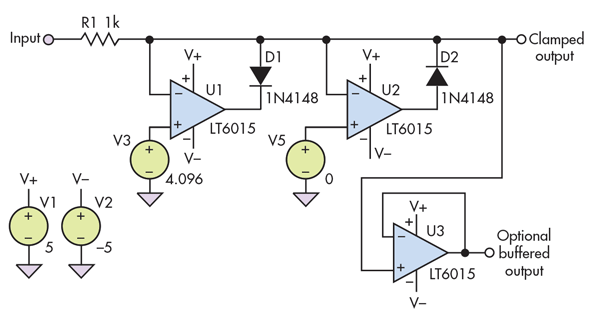
Figure 1. This clipping circuit uses a complementary pair of op amps to prevent excessive positive (U1) and negative signal excursions (U2) of the input signal, to maximum available signal dynamic range without damaging overload. Source: Electronic Design.

A simple op-amp clipper (Fig. 1) prevents these problems. The maximum allowable input voltage is applied to the non-inverting input of U1, and the output is fed back to the inverting input via small-signal diode D1. The ADC’s reference voltage can be used for the clipping reference if available. When the input voltage is below the reference, U1’s output is driven to the positive rail and D1 is reverse-biased, so the input signal passes through without being altered.

When the input goes above the clamp voltage, the op-amp output reverses and closes the loop through D1. As a result, it effectively becomes a unity-gain follower to the clamp voltage. Input resistor R1 limits the amount of current the op-amp output has to sink. A second op amp (U2) performs the complementary negative clipping function, preventing the signal from going below ground. Thus, in this example, the output signal is restricted to 4.096 V to 0 V out.

The article goes on to explain some of the unique challenges this circuit presents to the op-amp regarding the back-to-back diodes across their inputs. There are also considerations for slew-rate which affects the maximum frequency of operation and rail-to-rail operation. The article is worth a read.
enter image description here

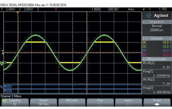
Figure 2. With the LT6015 and bipolar 10-V supplies, the circuit clamps a 7 V p-p sine wave at 0 and +4 V. (Same source as Figure 1.)


Can this be used in the earlier sections?

Probably a bad idea.
enter image description here

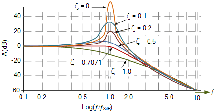
Figure 3. Various 2nd-order filter responses. Source: Electronics Tutorials.

Depending on your low-pass filter frequency response you may have a peak at the pole and this would result in a higher output voltage than your clipper. See the linked article for more.

\$\endgroup\$
16
  • \$\begingroup\$ +1 for cute use of op-amps. Only issue I can see is one of the op-amps failing could put whatever rail out to the output. But that comes under the category of fault limitation so is a different question ;) \$\endgroup\$
    – Trevor_G
    Commented Oct 21, 2017 at 16:18
  • \$\begingroup\$ Can this be used in the earlier sections? \$\endgroup\$ Commented Oct 21, 2017 at 16:20
  • \$\begingroup\$ Also the reason I am using two op-amps for stage 1-2 is because I want to use smaller resistances for variable gain (which can go up to 15x) which can't be used if I am using a resistance of 84k*15 (too high!) \$\endgroup\$ Commented Oct 21, 2017 at 16:21
  • \$\begingroup\$ @ZaidAlShattle you want to limit it later not earlier. The earlier you limit the smaller the values and the more the tolerances affect the values relative to your signal. Over value signals will not adversely affect the op-amps. \$\endgroup\$
    – Trevor_G
    Commented Oct 21, 2017 at 16:23
  • 1
    \$\begingroup\$ @Trevor: He's using the output of the second-last stage and an inversion of it so I think we can call that differential. \$\endgroup\$
    – Transistor
    Commented Oct 21, 2017 at 16:28
2
\$\begingroup\$

EEK 741s...

You can add either limiting diodes or zeners to the circuit but be aware that may change the linearity a little.

The question you have to ask is will the input itself survive a voltage greater than the ADC reference value. If the answer is yes, then limit it to under the max voltage it can take. Possibly with a forward pointing Zener over R10. You should also make sure the thing can never go negative (whatever the input can handle) either.

More often it is prudent to back off on the gain so your input to the ADC is a little less than maximum for the normal signal range. While doing that is it often convenient to chose a maximum value that is convenient from a human perspective. For example max value = 1000 for a 1024 bit DAC.

Note: If your max value is your normal max input then you will never know if it is actually over that.

NOTE 2: You want to add your limiting after all the amplification stages. If you try to do it earlier the values become so low that the tolerances involved swamp the signal. The op-amps themselves will not care much if the signal is too strong unless it reaches the rail. At that point you may get a lot of distortion.

\$\endgroup\$

Your Answer

By clicking “Post Your Answer”, you agree to our terms of service and acknowledge you have read our privacy policy.

Not the answer you're looking for? Browse other questions tagged or ask your own question.