0
\$\begingroup\$

I am part of a project that is implementing a power storage system. The storage device voltage must be monitored in order to direct power. The storage device voltage should remain between 12 and 36 V. The project uses a TI TMS320F28027 MCU which operates at 3.3 V. How can the 12 to 36 V be mapped onto 0 to 3.3 V for the MCU.

I posted a similar question here but it specified that the voltage would range from 0 to 60 V. The difference for this question is how to bias the voltage appropriately.

I also posted another question about biasing the output of a current sensor for an ADC, but it involved biasing a balanced voltage around 0 V. I am having trouble adapting the answer to this problem. Diagram from answer:
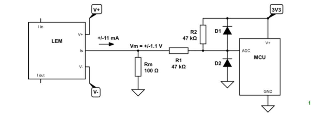
diagram from answer
Figure 1. Diagram from previous answer

An attempt to emulate the design methodology would be:

24 V maps to 1.65 V
38 V maps to 3.3 V
10 V maps to 0 V

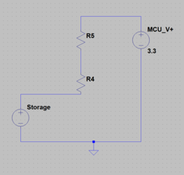
The most basic circuit model:

enter image description here

How to design the bias?

\$\endgroup\$
6
  • \$\begingroup\$ Is a negative voltage rail available this time? \$\endgroup\$
    – Transistor
    Commented Feb 10, 2018 at 0:37
  • \$\begingroup\$ yes there is a negative rail \$\endgroup\$
    – rur2641
    Commented Feb 10, 2018 at 0:44
  • \$\begingroup\$ Are you going to share the voltage? \$\endgroup\$
    – Transistor
    Commented Feb 10, 2018 at 0:45
  • \$\begingroup\$ the dual supply source is XP Power IZ2415S, it can supply +/- 100 mA at +/- 15 V. There are 2 LEM LAH 100-P sensors running of the source. They each draw 10 mA in addition to 1/2000 of the current sensed. They are each expected to sense an average of + 70 A which amounts to 90 mA total. I don't know what is meant in the power source datasheet by +/- 100 A. \$\endgroup\$
    – rur2641
    Commented Feb 10, 2018 at 1:12
  • \$\begingroup\$ Is your power system DC or AC??? I would expect AC from your \$\pm 11\:\text{mA}\$ on the schematic. But I expect DC from your statement that \$10\:\text{V}\$ should map to \$0\:\text{V}\$ (because, otherwise, what should \$-10\:\text{V}\$ and \$-38\:\text{V}\$ map to??) So what is the deal? Is this an AC system or a DC system. I'm confused. Also, it appears you have two questions -- (1) mapping the system voltage to within the ADC range; and (2) mapping the Hall Effect sensor range to with a similar ADC range. .... I admit, I'm confused right now. What exactly are you doing/asking? \$\endgroup\$
    – jonk
    Commented Feb 10, 2018 at 6:42

3 Answers 3

1
\$\begingroup\$

Rearranging:

  • 38 V maps to 3.3 V
  • 24 V maps to 1.65 V
  • 10 V maps to 0 V

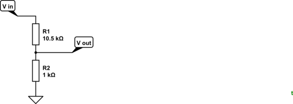
schematic

simulate this circuit – Schematic created using CircuitLab

Figure 1. An 11.5:1 potential divider.

The simplest solution is to use a potential divider with a ratio of 38:3.3 or 11.5:1. This would result in:

  • 38 V maps to 3.3 V
  • 24 V maps to 2.08 V
  • 10 V maps to 0.868 V

The 0.868 V offset can be removed in software. Again, you lose a little resolution with this approach.

If a negative voltage supply is available then the offset can be removed.

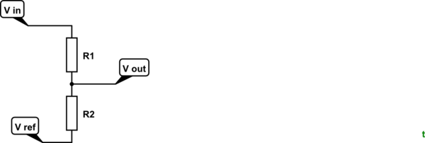
schematic

simulate this circuit

Figure 2. With a negative rail available the offset at minimum input voltage can be removed.

How:

  • The span is 38 - 10 = 28 V.
  • This has to be scaled to 3.3 V so a divider ratio of 28 / 3.3 = 8.5:1. Let's use 7.5k and 1k to give us the required ratio.

Now we need to figure out the negative reference voltage.

  • At 10 V in Vout will be 0 V. With the 8.5:1 ratio we will need to hold Vref at \$ - \frac {1}{8.5} 10 = -1.18 V \$.

So, R1 = 7.5k, R2 = 1k, Vref = -1.18 V should do the trick.

I'll leave it to you to work out how to create the reference voltage.

\$\endgroup\$
1
\$\begingroup\$

"Mapping" is a good description, but level shifting is mostly what is needed. If you source voltage is 12 volts to 36 volts (n), then use n/10 to get 1.2 volts to 3.6 volts. Subtract 1.2 volts to get 0 - 2.4 volts.

Use an op-amp with a gain of 1.375 to get a range of 0 to 3.3 volts. An op-amp with a negative supply of -3.3 volts will allow an output as low as zero volts

\$\endgroup\$
1
\$\begingroup\$

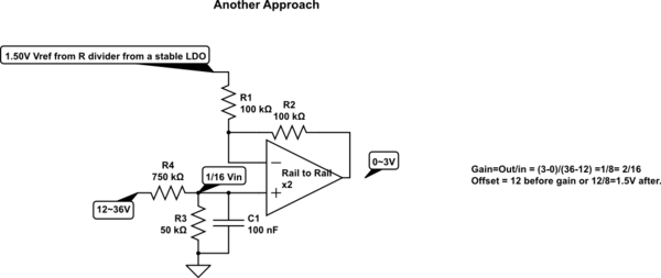
schematic

simulate this circuit – Schematic created using CircuitLab

\$\endgroup\$

Your Answer

By clicking “Post Your Answer”, you agree to our terms of service and acknowledge you have read our privacy policy.

Not the answer you're looking for? Browse other questions tagged or ask your own question.