3
\$\begingroup\$

This question and the answers hits close to the topic. One picture shows it as SOD. Silicon-oxide dielectric?

I'm aware that around/within the transistor, silicon oxide is grown for insulation where needed, but I can't seem to find clarity on the insulators surrounding the metal wire layers. Is it the same silicon dioxide?

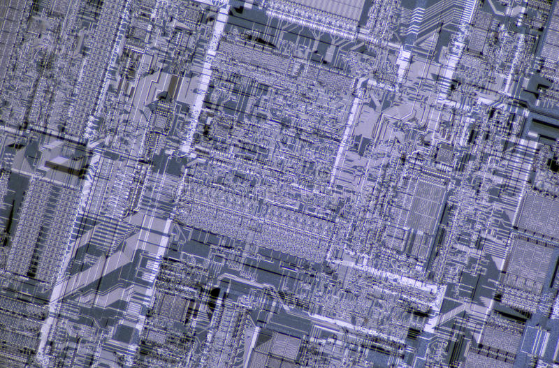
I ask because I wondered how we can see many of the details of the integrated circuit when there should be something insulating and physically supporting each metal wire layer. This means it's either clear or the layers are so thin that most of the light passes through anyway (likely both). SiO2 would fit the characteristics observed, but is that correct?

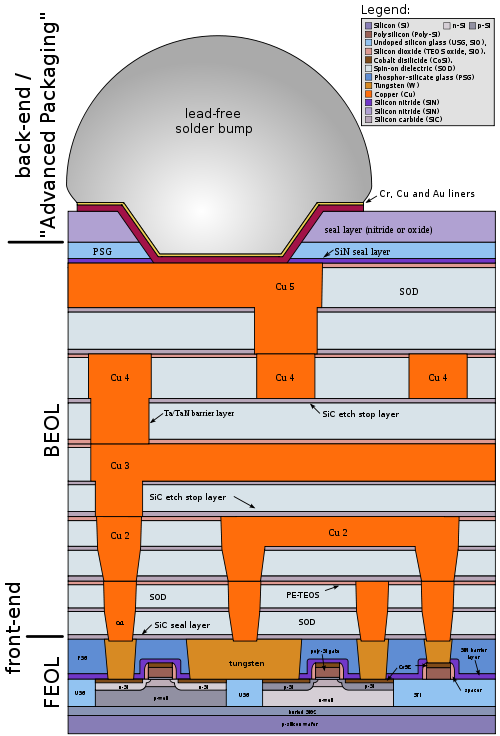
IC diagram IC image

\$\endgroup\$
1
  • 2
    \$\begingroup\$ The legend in your image says that SOD stands for "spin-on dielectric". Which gives you something to google to find out more. \$\endgroup\$
    – The Photon
    Commented Apr 25, 2018 at 18:26

3 Answers 3

1
\$\begingroup\$

From The Photon's observation and a little more research, the dielectric can come from a whole host of possible options. From here, it appears spin-on dielectrics can vary from organic based insulators/dielectrics to silicon based dielectrics. Most of the knowledge in this area appears locked away in published papers and as company specific IP.

From the link, some examples of polymer based insulators are polyimide, polynorbornenes, benzocyclobutene, and PTFE while silicon based spin-on dielectrics can be hydrogen silsesquioxane (HSQ) and methylsilsesquioxane (MSQ).

\$\endgroup\$
6
  • 1
    \$\begingroup\$ “Locked-away” in published papers is an oxymoron. Before the internet that was the gold standard of “making information public.” \$\endgroup\$ Commented Feb 5, 2019 at 15:29
  • \$\begingroup\$ @EdgarBrown Could be. Unless there's a paywall blocking easy access to that published information. \$\endgroup\$
    – horta
    Commented Feb 5, 2019 at 16:44
  • 1
    \$\begingroup\$ “Paywalls” are an artifact of the web era, before that (as now) all you needed is a public-access library, a photocopy card, and working legs. It is in the web era that public access is equated to “keeping my behind on my chair.” \$\endgroup\$ Commented Feb 5, 2019 at 16:57
  • \$\begingroup\$ @EdgarBrown Doesn't that assume that your library of choice actually has a subscription to that paywall? \$\endgroup\$
    – horta
    Commented Feb 5, 2019 at 17:03
  • 1
    \$\begingroup\$ Or is part of a library system that has some sort of agreement with the publisher. But so what? You are not the one paying and someone has to pay for the information being created in the first place. The immense majority of the international standards that underpin our civilization have to be bought (and can be quite expensive), that does not make them any less “public.” \$\endgroup\$ Commented Feb 5, 2019 at 17:12
1
\$\begingroup\$

In addition to @horta's answer regarding spin-on dielectrics and the thermal oxides grown in typical Silicon foundries, dielectrics are often deposited though vapor deposition techniques (e.g. MOCVD, PECVD). For example, silicon nitride is typically the inter-layer dielectric used for many GaAs and GaN processes.

These dielectrics are all mostly transparent in the optical spectrum (SiO2/TEOS, SiN, BCB, PI, etc.), so regular microscopy techniques will be able to resolve detail in most layers of the IC where no metals are deposited. A counterexample is BCB: BCB is quite opaque to wavelengths in the UV spectrum, and images of a wafer coated in BCB with a UV source and detector will not look like much.

\$\endgroup\$
3
  • \$\begingroup\$ Even metals are relatively transparent at some of these thicknesses. \$\endgroup\$ Commented Feb 5, 2019 at 15:31
  • \$\begingroup\$ @EdgarBrown For my education, do you have any specific examples? In my field, we typically don't see metals thinner than 0.3 microns or so. \$\endgroup\$
    – Shamtam
    Commented Feb 5, 2019 at 16:40
  • \$\begingroup\$ Transparency is relative, even 0.1% transmittance can be a problem in some designs, that could happen even at 0.1um. (springer.com/cda/content/document/cda_downloaddocument/…). (physics.stackexchange.com/questions/31830/…) \$\endgroup\$ Commented Feb 5, 2019 at 16:53
1
\$\begingroup\$

Si forms an insulating layer of SiO2 by thermal oxidation. This layers is a native oxide and the thickness is controlled by diffusion. I.e. self-limiting oxidation... The thickness thermally oxidized layers follows the Deal-Grove model. Deal and Grove developed this model while working at Fairchild semiconductor. Their work in thermal oxidation of Si was instrumental in facilitating the development of MOFSET devices that followed.

\$\endgroup\$

Your Answer

By clicking “Post Your Answer”, you agree to our terms of service and acknowledge you have read our privacy policy.

Not the answer you're looking for? Browse other questions tagged or ask your own question.