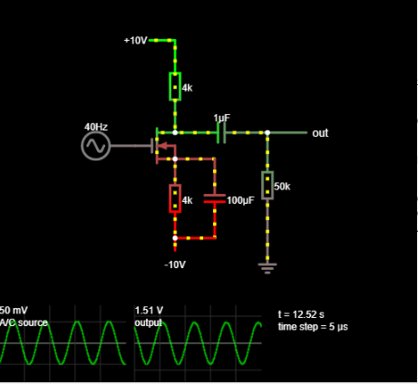
\$g_{m}\$ is indeed an important value when you are designing an amplifier, not only does it dictate the gain but also the bandwidth, noise performance, and linearity of the circuit. When we place a resistor from source to ground, we decouple ourselves from the intrinsic \$g_{m}\$ of the FET so while still important, it becomes little a less relevant because we no longer have a 1 to 1 dependency on it.
I'm going to try to explain \$g_{m}\$ in terms of MOSFET characteristics first and then I'll move to a small design example see (Design example below)
gm in terms of MOSFET parameters
For a N-channel MOSFET in saturation region, the drain current can be defined as:
\$I_{D} = \frac{1}{2} \mu_{n}C_{ox}\frac{W}{L}(V_{GS} - V_{th})^2(1 + \lambda V_{DS})\$
For simplicity let's assume that the channel length modulation \$\lambda = 0\$ thus
\$I_{D} = \frac{1}{2} \mu_{n}C_{ox}\frac{W}{L}(V_{GS} - V_{th})^2\$
Now, the transconductance \$g_{m}\$ for a MOSFET is defined as the change in drain current \$I_{D}\$ with respect to input voltage \$V_{GS}\$:
\$g_{m}=\frac{\delta I_{D}}{\delta V_{GS}} = \mu_{n}C_{ox}\frac{W}{L}(V_{GS} - V_{th})\$
After some algebraic manipulation, \$g_{m}\$ can also be written as:
\$g_{m}=\sqrt{2\mu_{n}C_{ox}\frac{W}{L}I_{D}}=\frac{2I_{D}}{V_{GS} - V_{th}}\$
Where:
- W: Width of transistor (you can control this if you are designing the IC)
- L: Length of transitor (you can control this if you are designing the IC)
- \$\mu_{n}C_{ox}\$: Are the mobility and the oxide capacitance respectively
(assume constant)
- \$V_{GS}\$: the gate to source voltage
- \$V_{th}\$: the threshold voltage (assume constant)
So unless you are designing the IC and have control over \$\frac{W}{L}\$, the only "knobs" you can control are the DC operation point \$I_{D}\$ & \$V_{GS}\$. Once these two parameters are set, the \$g_{m}\$ is pretty much set for that \$I_{D}\$, \$V_{GS}\$ combination.
Now, as far as the small signal gain of the circuit is concerned , the output voltage \$v_{out}\$ can be defined as: (using lower case variables to refer to small signal)
Assuming the source resistance is zero to simplify the analysis
\$v_{out}\$ = \$i_{D}R_{eq}\$
Where \$R_{eq}\$ is the total equivalent resistance at the output:
\$R_{eq} = R_{Drain} || R_{Load} || r_{o}\$
where \$r_{o}\$ is the output resistance of the transistor in saturation region which you can assume to be large. Assuming \$R_{Drain} << R_{Load} << r_{o}\$
\$R_{eq} \approx R_{Drain}\$
thus
\$v_{out}\$ = \$i_{D}R_{Drain}\$
defining the small signal transconductance as
\$g_{m}=\frac{i_{D}}{v_{GS}}\$
rearranging
\$i_{D}=-g_{m}v_{GS}\$, where \$v_{GS}\$ is your input AC voltage
bringing everything together, the voltage gain can be defined as:
\$\frac{v_{out}}{v_{in}}=A_{v}=-g_{m}R_{Drain}\$
What happens when we have a resistor connected from source to ground
When we put a resistor at the source terminal we introduce local feedback which reduces the \$g_{m}\$ but increases the linearity of the circuit in a process called "source degeneration". By analyzing the small circuit equivalent we end up with:
\$g_{m} \approx -\frac{1}{R_{Source}}\$
So the gain \$A_{v}\$ can be expressed as:
\$\frac{v_{out}}{v_{in}}=A_{v}=-\frac{R_{Drain}}{R_{Source}}\$
Now you have more control of the gain and linearity of the circuit.
Design example
Say, you were to design a stand alone amplifier, and you have a target gain of 10 V/V and this gain is dictated by amplification needed, noise level, etc. Thus:
\$A_{v}=-g_{m}R_{Drain} = 10\$
for the MOSFET to be in saturation, we need \$V_{DS} > V_{GS} - V_{th}\$ and the higher \$V_{DS}\$ the better linearity we get from our circuit. However, there's never free lunch, the higher the \$V_{DS}\$, the smaller the \$v_{out}\$ can swing in the positive direction without hitting the supply. So to be conservative lets say you set your \$V_{DS} = 200mV\$. Now what happens if \$V_{out}\$ swings \$100mV\$ in the negative direction? That will reduce our \$V_{DS} = 200mV\$ to \$100mV\$ and we risk leaving the saturation region. Since we know the swing requirement for \$V_{out}\$, we can add a \$100mV\$ margin to provide some headroom. Now:
\$V_{DS} = 300mV\$
\$R_{Drain} = \frac{V_{DD} - V_{DS}}{I_{D}}\$
As a rule of thumb and in the interest of linearity, the DC bias current \$I_{D}\$ can be set as
\$I_{D} = 10\times i_{D}\$ where \$i_{D}\$ is the ac output current we are trying to deliver.
Now you have all the values you need to start your design. Notice though that our design heavily depends on \$g_{m}\$ which varies across temperature and unless we are designing the IC, we have little control over.
Having precise control over \$g_{m}\$ might or might not be an issue but that's why people use the source resistance \$R_{Source}\$ to rely on the ratio of two resistors rather than the internals of the FET. So when we take this approach we don't really need to worry much about the value of \$g_{m}\$.


