5
\$\begingroup\$

If I place my decoupling capacitor (more or less) like shown in the figure: enter image description here
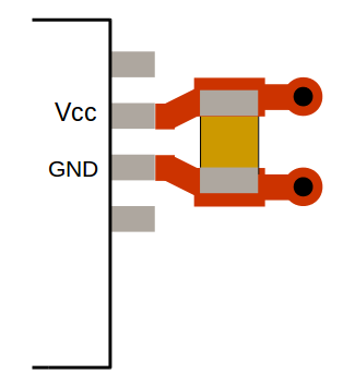
I wonder: can the vias be inside the pads? (one via inside each).

Two advantages I can see are: (1) we avoid the inductance of the trace from the capacitor pad to the via, since we eliminate that trace. And (2) we save space on the board.

One inconvenience I can see is that it will disrupt the estimates of the amount of solder paste one has to place. For "manual" reflow solder projects, one can certainly compensate for it. Is this a real problem for automated soldering/assembly setups?

Are there any other reasons to avoid this? (seems like an interesting trick with certain advantages --- the fact that I can't find a single reference to it when searching online tells me that there's probably some fundamental reason why this should not be done)

\$\endgroup\$
4
  • 3
    \$\begingroup\$ It is called "via in pad" and is "only" a manufacturing issue. See: community.cadence.com/CSSharedFiles/forums/storage/27/1324522/… and blog.screamingcircuits.com/via_in_pad \$\endgroup\$
    – filo
    Commented Aug 1, 2018 at 20:48
  • 1
    \$\begingroup\$ related: Anything bad to place a via on a pad? \$\endgroup\$ Commented Aug 1, 2018 at 21:25
  • \$\begingroup\$ could perhaps move the vias to between the capacitor and the chip \$\endgroup\$ Commented Aug 2, 2018 at 8:24
  • \$\begingroup\$ @jasen -- yes, I've seen that technique. Aside from the fact that it baffles me why that approach works, w.r.t. my question it doesn't make a difference: the extra required space to the right of the capacitor now moves to the left of the capacitor. For a particular layout, depending on other required traces or parts, the approach you describe may be the one that works w.r.t. space usage. \$\endgroup\$
    – Cal-linux
    Commented Aug 2, 2018 at 20:08

1 Answer 1

3
\$\begingroup\$

You are correct about the advantages of lower inductance and saving space. However, via in pad adds cost to the fabrication of PCB because it requires that that the via be filled and capped to maintain a flat continuous SMT pad.

\$\endgroup\$
1
  • 5
    \$\begingroup\$ Besides the added costs of via-in-pad, there is a good chance that the planarity of the pad is compromised even if via-in-pad is a supported process, even well controlled processes are subject to solder creep through the via, and would require you to dictate the reflow very carefully. SMT Ceramics Capacitors are susceptible to mechanical cracking (and subsequent failure) when mounted on non-flat surfaces or other defects that cause the mounting head to apply excess force across the smt part. They are more brittle than typical SMT IC's and resistors. \$\endgroup\$
    – crasic
    Commented Aug 1, 2018 at 20:42

Your Answer

By clicking “Post Your Answer”, you agree to our terms of service and acknowledge you have read our privacy policy.

Not the answer you're looking for? Browse other questions tagged or ask your own question.