1
\$\begingroup\$

I've been trying to research how a class C amplifier works, and it makes perfect sense to me, but I'm having problems getting it to function in LTSpice. I have the latest LTSpice version (XVII with latest updates as of last week).

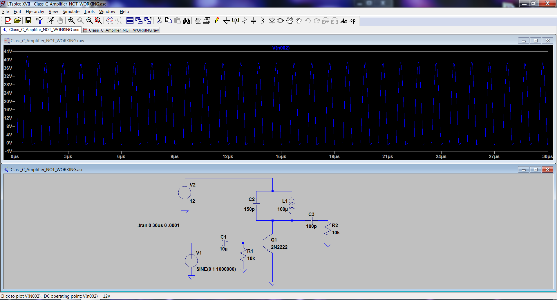
I can't seem to get my "resonant network" to resonate with a sine wave, no matter what I keep getting this cut off wave. What am I doing wrong ?

I have done a lot of searching on the web and this seems like the proper circuit structure - and I think it would probably work in real life, but in LTSpice it indicates it isn't going to work and I can't see why.

Trying to amplify a simple 1Mhz carrier sine signal here.

Here is a picture of the circuit. The waveform is being sampled from the collector of the transistor

enter image description here

Since I can't figure out how to share or attach a file, here is the LTSpice *.asc file contents

Version 4
SHEET 1 1076 680
WIRE 240 -128 -192 -128
WIRE -192 -96 -192 -128
WIRE 240 -64 240 -128
WIRE 240 -64 160 -64
WIRE 336 -64 240 -64
WIRE 160 -32 160 -64
WIRE 336 -32 336 -64
WIRE -192 32 -192 -16
WIRE 160 80 160 32
WIRE 240 80 160 80
WIRE 336 80 336 48
WIRE 336 80 240 80
WIRE 400 80 336 80
WIRE 512 80 464 80
WIRE 240 144 240 80
WIRE -32 192 -160 192
WIRE 96 192 32 192
WIRE 176 192 96 192
WIRE 512 192 512 160
WIRE 96 208 96 192
WIRE -160 240 -160 192
WIRE 96 320 96 288
WIRE -160 352 -160 320
WIRE 240 384 240 240
FLAG 96 320 0
FLAG -160 352 0
FLAG 240 384 0
FLAG -192 32 0
FLAG 512 192 0
SYMBOL npn 176 144 R0
SYMATTR InstName Q1
SYMATTR Value 2N2222
SYMBOL res 80 192 R0
SYMATTR InstName R1
SYMATTR Value 10k
SYMBOL cap 32 176 R90
WINDOW 0 0 32 VBottom 2
WINDOW 3 32 32 VTop 2
SYMATTR InstName C1
SYMATTR Value 10µ
SYMATTR SpiceLine V=6.3 Irms=0 Rser=0.001 Lser=0 mfg="TDK"   pn="C3216X5ROJ106M" type="X5R"
SYMBOL voltage -160 224 R0
WINDOW 123 0 0 Left 0
WINDOW 39 0 0 Left 0
SYMATTR InstName V1
SYMATTR Value SINE(0 1 1000000)
SYMBOL voltage -192 -112 R0
WINDOW 123 0 0 Left 0
WINDOW 39 0 0 Left 0
SYMATTR InstName V2
SYMATTR Value 9
SYMBOL ind2 352 64 R180
WINDOW 0 36 80 Left 2
WINDOW 3 36 40 Left 2
SYMATTR InstName L1
SYMATTR Value 100µ
SYMATTR Type ind
SYMATTR SpiceLine Ipk=0.04 Rser=11 Rpar=78263 Cpar=1.868p mfg="Würth Elektronik" pn="74476420 WE-GF 1210"
SYMBOL cap 176 32 R180
WINDOW 0 24 56 Left 2
WINDOW 3 24 8 Left 2
SYMATTR InstName C2
SYMATTR Value 150p
SYMATTR SpiceLine V=6.3 Irms=3.93m Rser=19.9098 Lser=0
SYMBOL res 496 64 R0
SYMATTR InstName R2
SYMATTR Value 220
SYMBOL cap 464 64 R90
WINDOW 0 0 32 VBottom 2
WINDOW 3 32 32 VTop 2
SYMATTR InstName C3
SYMATTR Value 470p
SYMATTR SpiceLine V=50 Irms=20.8m Rser=5.448 Lser=0
TEXT -424 104 Left 2 !.tran 0 30us 0 .0001
\$\endgroup\$
10
  • \$\begingroup\$ I have a tremendous fund of ignorance about Class-C amplifiers but doesn't 150 pF and 100 µH resonate at 1.3 MHz? \$\endgroup\$
    – Transistor
    Commented Aug 10, 2018 at 21:47
  • \$\begingroup\$ @Transistor yes, I also "stepped" the capacitor value in the LC circuit and never found a value that gave me a sine wave. \$\endgroup\$
    – niko20
    Commented Aug 10, 2018 at 21:56
  • 2
    \$\begingroup\$ I am not an expert on class C amplifiers either, but this says that clipping half the cycle of the output is expected behavior. (notice the mention of a "suitable tuned load" toward the bottom of the page) \$\endgroup\$
    – The Photon
    Commented Aug 10, 2018 at 22:12
  • \$\begingroup\$ @ThePhoton yes , it is expected. How Class C works is the LC network in the collector is supposed to then "ring" and basically reformulate the original sine wave. That's why Class C amplifiers are so efficient, they only stay on a short part of the cycle. Then you have LC networks to "filter" and form the clean sinewave output. This circuit is pretty much textbook of how Class C amplifiers are presented, but yet it doesn't seem to work..I have lots of trouble with LTSpice lately argh! \$\endgroup\$
    – niko20
    Commented Aug 10, 2018 at 22:16
  • 2
    \$\begingroup\$ A pretty good model of these hard-driven amplifiers is a fast switch that shorts the resonator to ground for a short period (perhaps up to half a cycle). Yes, the collector waveform isn't a pretty sinusoid, and multipole lowpass/bandpass filters are needed to suppress harmonics sufficiently. That approach is often taken. Beware - filters are analyzed with SPICE's AC analysis (which is entirely linear), but the switch model is not-at-all a linear signal source. \$\endgroup\$
    – glen_geek
    Commented Aug 10, 2018 at 23:34

5 Answers 5

2
\$\begingroup\$

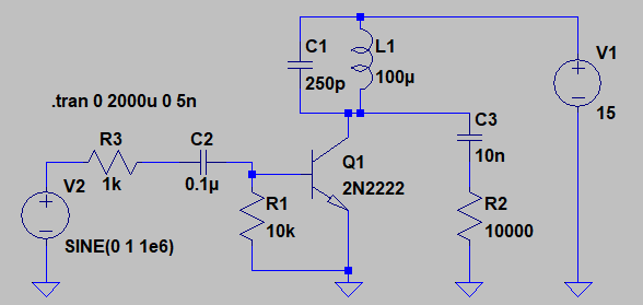
Essentially the same Class-C type circuit with a few component value changes, to achieve a somewhat-sinewave at the collector (your design goal).
Loaded resonator Q is about 15, so that the second-harmonic is suppressed by only 28 dB below the fundamental.

An added resistor (R3) decreases drive into the transistor base. DC supply has been increased slightly. L1 resonates with C1 near 1 MHz. Only 7.2 mW are delivered to the 10K load resistor R2. one-resonator class C driver

\$\endgroup\$
2
  • \$\begingroup\$ Wow that circuit puts out a nice clean signal. Thanks for hacking away at it. This should help me learn some things \$\endgroup\$
    – niko20
    Commented Aug 11, 2018 at 1:21
  • \$\begingroup\$ ok so I think my problems was I was thinking a Class C was "full on, full off" whereas from what I'm seeing from a circuit when it actually works in LTSpice, is that it's still in the linear region, just not very long. So it's not turning full ON , it's still crossing the linear range, but only for a very very short while and then it turns off again. So I was probably overdriving it, turning it full ON, which is more something you see in switch mode power supplies or class D amplifiers. Class C still stays in linear range but just for very short time \$\endgroup\$
    – niko20
    Commented Aug 11, 2018 at 1:46
1
\$\begingroup\$

Ok this is weird,

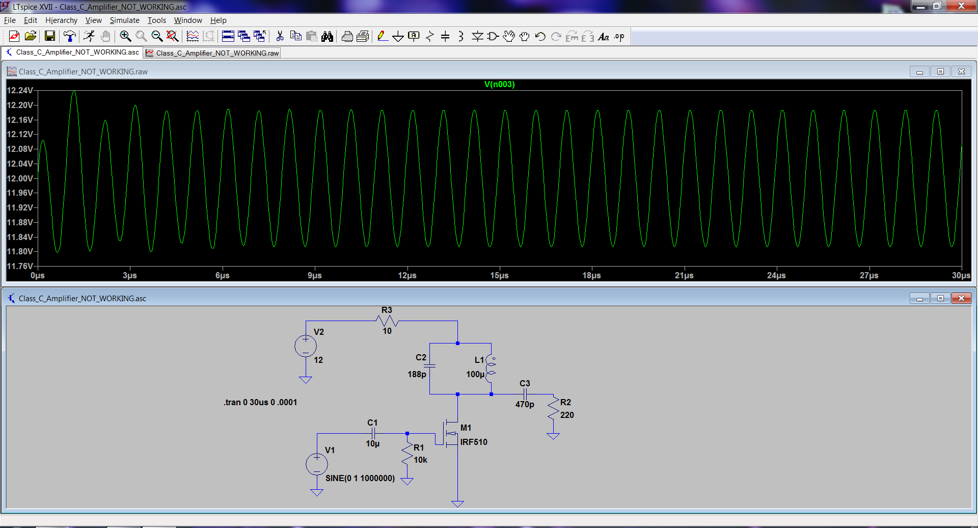
I replaced the 2N2222 with an IRF510 MOSFET and now the circuit seems to work.

NEVER MIND, THE IRF510 WAS NOT FULLY TURNING ON HERE

-- EDIT : It turns out, this probably was working after all after seeing the final posts and information from geek --

Maybe this is some sort of reverse voltage breakdown occurring in the 2N2222?

enter image description here

\$\endgroup\$
6
  • \$\begingroup\$ Bah nevermind, this was because my carrier was only 1V p-p so the mosfet wasn't fully turning on I don't believe. If I up the sine voltage to 6 volts I get the same bad waveforms as with the BJT. \$\endgroup\$
    – niko20
    Commented Aug 10, 2018 at 22:10
  • \$\begingroup\$ Notice your output amplitude is now only about 0.4 V peak-peak, not 40 V like before. It's a lot easier to keep a circuit linear with a smaller signal swing. \$\endgroup\$
    – The Photon
    Commented Aug 10, 2018 at 22:10
  • \$\begingroup\$ @ThePhoton ya..but actually, this isn't supposed to be linear. It's supposed to turn on HARD and then off, and the tuned circuit it supposed to fill in the rest. \$\endgroup\$
    – niko20
    Commented Aug 10, 2018 at 22:11
  • \$\begingroup\$ What do you measure across the load R2 ? \$\endgroup\$
    – Marla
    Commented Aug 10, 2018 at 22:20
  • \$\begingroup\$ @Marla it looks pretty much the same as the signal at the collector, but a slightly less voltage because the output capacitor cuts down the AC signal a small amount \$\endgroup\$
    – niko20
    Commented Aug 10, 2018 at 22:21
1
\$\begingroup\$

The transistor base emitter junction is a diode, or act as one as far as inputs to the base are concerned. On the positive signal peak you are charging up the capacitor C1, on the negative signal minimum the 10k resistor is too high valued to discharge the capacitor, it remains charged. On the next positive signal peak the base voltage won't exceed 0.7 volts to conduct again. The polarity of C1 is shown the wrong way round, relative to the charging effect. The 10 k resistor should be replaced with a radio frequency choke (RFC). Which is just an inductor. Or you can replace the 10k resistor with a signal diode the opposite way around from the base emitter diode.

\$\endgroup\$
0
\$\begingroup\$

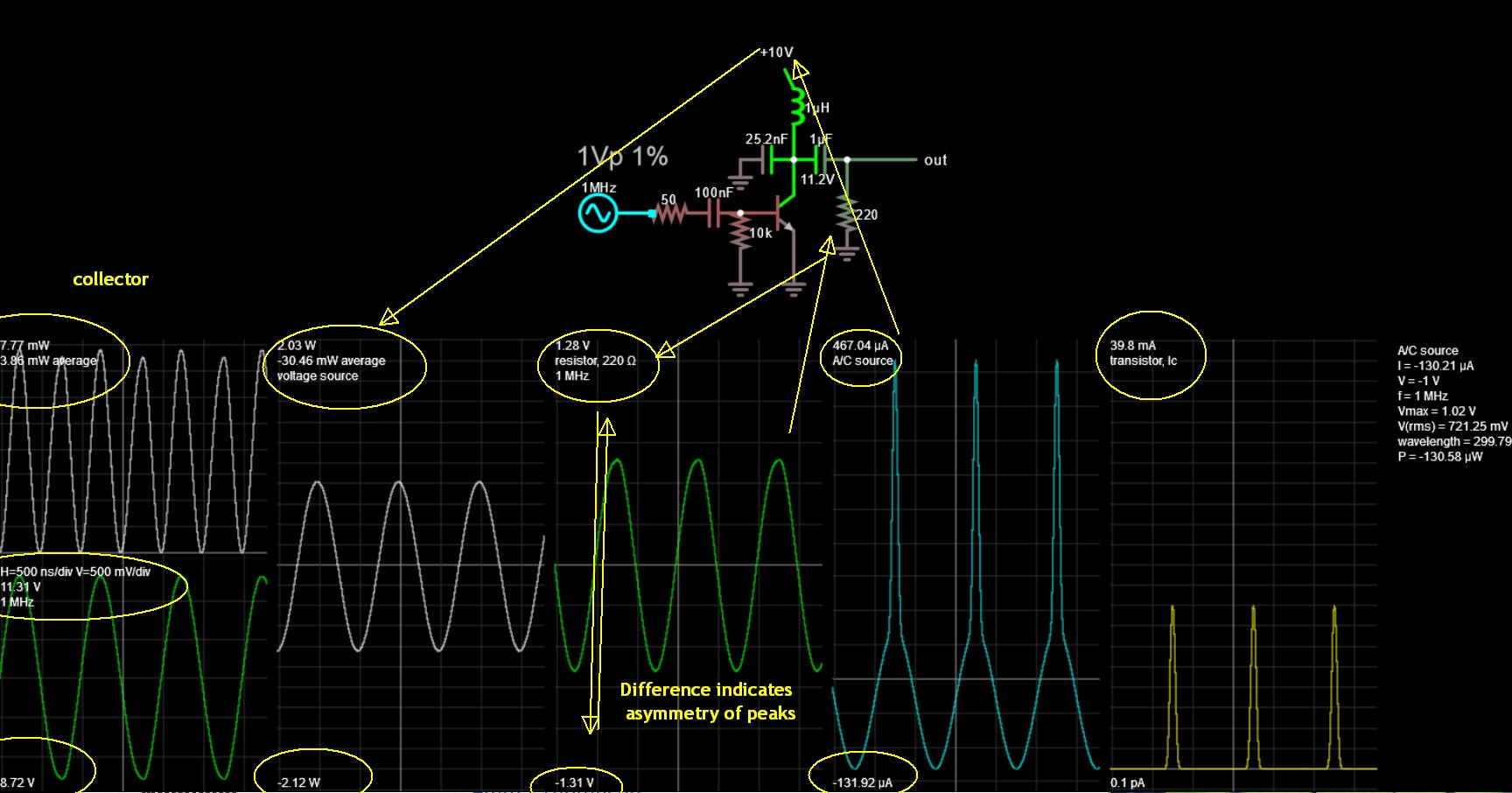
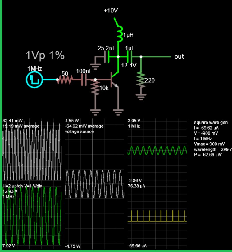
The input current and duty cycle is critical.
Below with a sine wave input at 1.02V and 50 Ohms enter image description here

I lowered tank circuit impedance by factor of 100 with 1uH and raised cap output to effects of f shift from duty cycle and thus amplitude. AC source is actually the DC supply current (Collector + resonator).

Load is 220 to reduce excess Q and get more power like into a long wire antenna.


Below is just a pulse input. enter image description here

With a sine wave current, the critical base current is

\$\endgroup\$
8
  • \$\begingroup\$ Wait a minute though, this is a Class - C amplifier. It's suppose to get starved. The LC network is supposedly then recovers the rest of the waveform (from the collapsing field), in other words, it should "ring"..but it's not ringing. \$\endgroup\$
    – niko20
    Commented Aug 10, 2018 at 21:57
  • \$\begingroup\$ What Rb. I can see R1. Also, class C requires zeron DC bias. \$\endgroup\$
    – Marla
    Commented Aug 10, 2018 at 22:01
  • \$\begingroup\$ I think you may be right Tony, I may be spending TOO much time in conduction. I accepted glen_geek's answer because his circuit seems to function correctly and I think part of his solution was to decrease the input value to allow the LC tank to function \$\endgroup\$
    – niko20
    Commented Aug 11, 2018 at 1:22
  • \$\begingroup\$ ok so I think my problems was I was thinking a Class C was "full on, full off" whereas from what I'm seeing from a circuit when it actually works in LTSpice, is that it's still in the linear region, just not very long. So it's not turning full ON , it's still crossing the linear range, but only for a very very short while and then it turns off again. So I was probably overdriving it, turning it full ON, which is more something you see in switch mode power supplies or class D amplifiers. Class C still stays in linear range but just for very short time \$\endgroup\$
    – niko20
    Commented Aug 11, 2018 at 1:44
  • \$\begingroup\$ Try reducing L to 1uH and scale up caps x100 \$\endgroup\$
    – D.A.S.
    Commented Aug 11, 2018 at 1:49
0
\$\begingroup\$

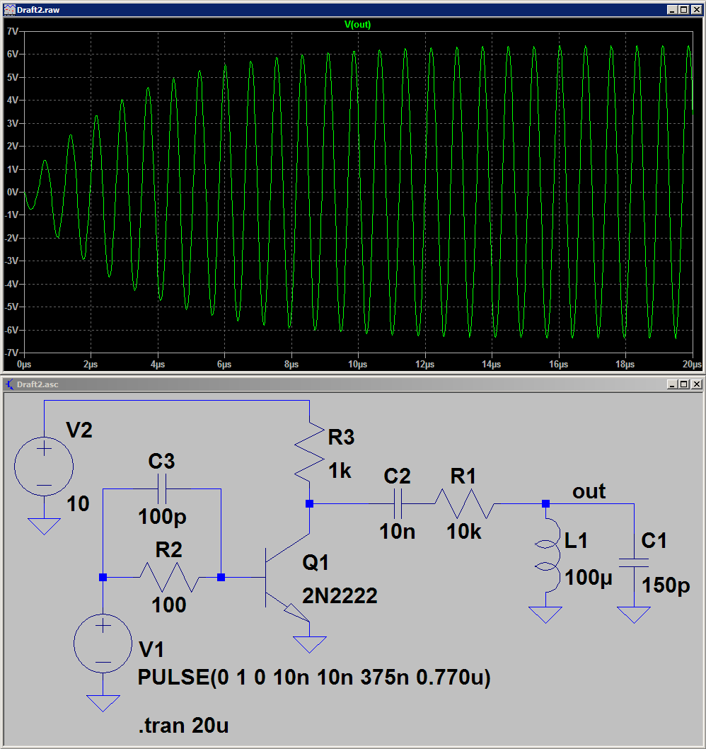
What you're getting is how a class-C amplifier works. You need additional filtering to get a nice looking sine wave.

Keep in mind that the bandwidth of a simple RLC circuit is \$ \frac{1}{2\pi RC}\ \$ (from the low-pass prototype of the BPF). When the transistor is off, your circuit has a bandwidth of \$ 106\;kHz = \frac {1}{2\pi (10k)(150p)} \$ (this assumes C3 is much larger to simplify the maths) which means you'll get a sine wave output.
When the transistor is switched on, R approaches zero which means the bandwidth will be very large and you will get a square wave on the lower part of the waveform. You are driving the tank circuit with apx 50% duty cycle.

If you want a sine wave on the output:
Option 1: If you make your input signal a 1% duty cycle rectangular waveform [PULSE(0 2 0 1n 1n 10n 0.769u)], you will better approximate a sine wave output with a small discontinuity in the output waveform. Additional filtering will give you a prettier waveform.

Option 2:
Make the resistance across the LC tank relatively constant, the bandwidth won't change significantly. However, this isn't a class-C amplifier.

enter image description here

\$\endgroup\$

Your Answer

By clicking “Post Your Answer”, you agree to our terms of service and acknowledge you have read our privacy policy.

Not the answer you're looking for? Browse other questions tagged or ask your own question.