0
\$\begingroup\$

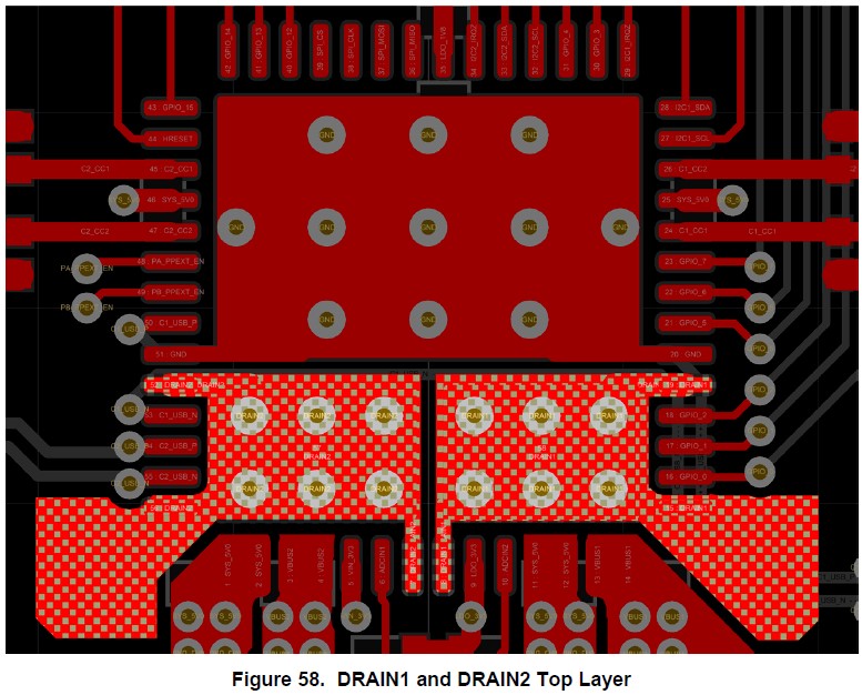
I'm designing a board around 2 Texas Instruments TPS65988. In the datasheet a layout example is shown where "fins" are placed around pads to provide further thermal dissipation. A pour to create this region sounds to me the best option to draw these regions. However, designing them with lines is very time consuming and not precise at all, even with a grid of 0.025mm setted in Altium, given the total dimensions of these fins (TPS65988 is a 7.15 x 7.15 mm QFN IC).

I tried to draw Solid Regions (faster to draw, more precise) but unfortunatelly I don't know how to exclude vias not connected to the same net of these fins from those solid regions (look at the bottom left via in picture below). It's very easy with Polygon Manager... But I can't find a easy way to do the same with solid regions.

So, my question is... How do they draw them? What is the best way to draw them in a fast and straighforward procedure?

enter image description here

\$\endgroup\$
5
  • \$\begingroup\$ "I don't know how to exclude vias not connected to the same net" This will be done by the tool when you pour a polygon and your Design Rules say to have X gap between polygons and unrelated nets. (I avoid specific terminology, since it's been a while since I played in Altium). \$\endgroup\$ Commented Feb 21, 2019 at 20:44
  • 1
    \$\begingroup\$ Solid regions just cover all the space inside them, they don't exclude vias or anything else. The ability to automatically pour around vias and other objects is exactly the advantage of using a polygon rather than a region. \$\endgroup\$
    – The Photon
    Commented Feb 21, 2019 at 22:32
  • \$\begingroup\$ 2nd, remember the physical edges of the copper can probably vary by at least 0.025 mm due to uncertainty about the etching speed, registration of the masks, etc. So trying to design things to the nearest micron is pointless. What you have in your picture looks pretty good to me. \$\endgroup\$
    – The Photon
    Commented Feb 21, 2019 at 22:36
  • \$\begingroup\$ @KevinKruse yes, I know! I was trying to understand if there was something like that also for solid regions. \$\endgroup\$
    – SashaLag
    Commented Feb 22, 2019 at 0:06
  • \$\begingroup\$ @ThePhoton thank you! Sometimes I forget about it. Anyway what I have in picture is from TI datasheet. I dream of having something like that also in my PCB. I will give polygon another shot then! \$\endgroup\$
    – SashaLag
    Commented Feb 22, 2019 at 0:06

2 Answers 2

1
\$\begingroup\$

Solid Regions are just that, solid; they do not obey clearance or connection rules, and are solid blobs of copper (or silkscreen, or soldermask opening, or..) merely checked against design rules.

The preferred way to do this is a Polygon, which will pour around the structures with specified clearance, and connecting as needed; and setting the connect rules as required. For example, you might set a PolygonConnect rule: InNetClass('Power'), connection direct, or at least wider/shorter spokes, etc. And set the relevant net(s) to the class (which should be done on the schematic with a class directive symbol).

It's a good idea in general to set a PolygonConnect rule, IsVia, direct connection (no spokes), so you don't have to worry about that gumming up the design either. (Vias never need spokes, by themselves, but pads -- and perhaps vias used as pads say as testpoints during development -- may want thermal relief for easier soldering.)

\$\endgroup\$
0
\$\begingroup\$

I would do as you first intended and use polygon pours - but instead of just one, I'd draw multiple smaller ones.

That makes it much easier to be fast and precise, as you can have a larger grid setting for most of the fills.

Otherwise, if you end up using a Solid Region, you will have to ensure your component is affected by the Design Rules properly.

\$\endgroup\$
0

Your Answer

By clicking “Post Your Answer”, you agree to our terms of service and acknowledge you have read our privacy policy.

Not the answer you're looking for? Browse other questions tagged or ask your own question.