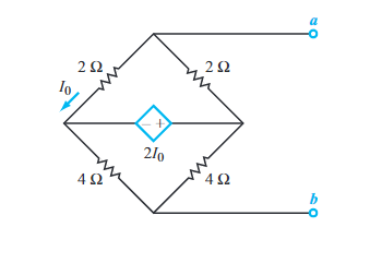
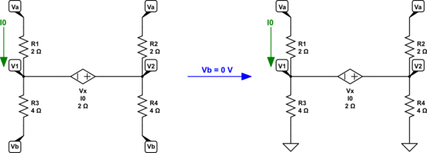
You really should use the schematic editor that exists here (CircuitLab) so that the parts in your schematic have labels that can be addressed and discussed more easily. Let's do that:

simulate this circuit – Schematic created using CircuitLab
On the left side is your schematic, slightly redrawn. On the right side is the same schematic, with the assignment of \$V_\text{b}=0\:\text{V}\$ (which we are allowed to do to exactly one and only one node of our choosing.) With the right side schematic, the equation development is slightly less tedious but results in the same answer, regardless.
You should readily understand that \$I_0=\frac{V_\text{a}-V_1}{R_1}\$, or put another way, that \$V_1=V_\text{a}-R_1\cdot I_0\$ (the value of \$V_\text{a}\$, less the voltage drop across \$R_1\$.) Also, it's not at all hard to realize that \$V_2=V_1+V_\text{x}\$, where \$V_\text{x}=2\:\Omega\cdot I_0\$. It follows that:
$$\begin{align*}
V_2&=V_1+V_\text{x}\\
&=\left(V_\text{a}-R_1\cdot I_0\right)+\left(2\:\Omega\cdot I_0\right)\\
&=\left(V_\text{a}-2\:\Omega\cdot I_0\right)+\left(2\:\Omega\cdot I_0\right)\\
&=V_\text{a}
\end{align*}$$
As \$V_2=V_\text{a}\$, there cannot be any current in \$R_2\$. Therefore, \$I_0\$ is the only current passing from \$V_\text{a}\$ to \$V_\text{b}\$ (though it takes two different paths in order to arrive at \$V_\text{b}\$ from \$V_\text{a}\$.) So \$R_\text{TH}=\frac{V_\text{a}-V_\text{b}}{I_0}\$ and in keeping with our tentative assignment (for these purposes) of \$V_\text{b}=0\:\text{V}\$, therefore: \$R_\text{TH}=\frac{V_\text{a}}{I_0}=\frac{V_\text{a}}{\frac{V_\text{a}-V_1}{R_1}}=R_1\cdot\frac{V_\text{a}}{V_\text{a}-V_1}\$.
Now you know that \$I_{R_4}=\frac{V_\text{a}}{R_4}\$ and all of \$I_{R_4}\$ must be the same as the current in \$V_\text{x}\$. The remainder is \$I_{R_3}=I_0-\frac{V_\text{a}}{R_4}\$ and therefore:
$$\begin{align*}
V_1&=R_3\cdot I_{R_3}\\
&=R_3\cdot\left(I_0-\frac{V_\text{a}}{R_4}\right)\\
&=R_3\cdot\left(\frac{V_\text{a}-V_1}{R_1}-\frac{V_\text{a}}{R_4}\right)\\\\
&\text{solving for }V_1,\\\\
V_1&=V_\text{a}\cdot \frac{\frac{1}{R_1}-\frac{1}{R_4}}{\frac{1}{R_1}+\frac{1}{R_3}}\\
&=\frac13\cdot V_\text{a}
\end{align*}$$
Finally,
$$R_\text{TH}=R_1\cdot\frac{V_\text{a}}{V_\text{a}-V_1}=R_1\cdot\frac{V_\text{a}}{V_\text{a}-\frac13\cdot V_\text{a}}=R_1\cdot\frac{1}{1-\frac13}=\frac32 R_1=3\:\Omega$$
I've taken a completely different approach than your mesh approach. Mostly, to avoid doing your homework for you. But partly to bend your mind in another direction to improve mental flexibility and partly to illustrate some other principles. (Re-drawing schematics to help change perspectives and assigning \$0\:\text{V}\$ to exactly one node, for example.)
There are many approaches to this problem. On that note, let's try a different perspective.
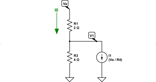
Now that we know that \$V_2=V_\text{a}\$, we can re-write the schematic:

simulate this circuit
The above schematic follows, logically. If \$V_2=V_\text{a}\$ and there's no current in \$R_2\$, then clearly \$I_{R_4}=\frac{V_\text{a}}{R_4}\$ is sinking current away from the \$V_1\$ node. (It subtracts from \$I_0\$.) So the above schematic is equivalent for analysis purposes.
Nodal analysis suggests \$\frac{V_1}{R_1}+\frac{V_1}{R_3}+\frac{V_\text{a}}{R_4}=\frac{V_\text{a}}{R_1}\$ and therefore: \$V_1=V_\text{a}\left(\frac{1}{R_1}-\frac{1}{R_4}\right)\left(R_1\mid\mid R_3\right)\$. (Feel free to do the algebra.) We know that \$R_\text{TH}=\frac{V_\text{a}}{I_0}\$ and that \$I_0=\frac{V_1}{R_3}+\frac{V_\text{a}}{R_4}\$. So:
$$\begin{align*}
R_\text{TH}&=\frac{V_\text{a}}{I_0}=\frac{V_\text{a}}{\frac{V_1}{R_3}+\frac{V_\text{a}}{R_4}}\\\\
&=\frac{V_\text{a}}{\frac{V_\text{a}\left(\frac{1}{R_1}-\frac{1}{R_4}\right)\left(R_1\mid\mid R_3\right)}{R_3}+\frac{V_\text{a}}{R_4}}\\\\
&=\frac{1}{\frac{\left(\frac{1}{R_1}-\frac{1}{R_4}\right)\left(R_1\mid\mid R_3\right)}{R_3}+\frac{1}{R_4}}\\\\
&= 3\:\Omega
\end{align*}$$
Just another way to confirm the earlier result.

