There is a gotcha when measuring supply voltage ripple: it depends on load current.
For an oldschool transformer-rectifiers-capacitor supply, more load current increases ripple voltage.
For a switching converter, it is more complicated. Quite often, wall wart AC-DC switching converters will be optimized for low idle current at no load, as people often leave them plugged in with no load attached. This often happens with cellphone chargers. In this situation, the converter spends most of the time in sleep mode doing nothing, and only recharges the output capacitor once in a while when its voltage is below a threshold, then it goes back to sleep mode. This results in a sawtooth ripple on the output, and this is most likely what makes your multimeter display those weird readings.
But as soon as you connect a load, the converter will work continuously, which results in a different ripple voltage value and frequency. So, don't trust your multimeter measurements too much. Also a multimeter won't tell you about the high frequency noise.
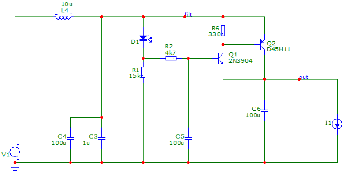
Anyway. If you want a tracking regulator which cleans up noise while allowing you to adjust voltage with the voltage control on your wall wart, you can try a capacitance multiplier like this (fancy version):

The LC filter at the input rejects HF. Then there is a lowpass, and a follower, to reject LF ripple. I used a CFP follower for lower output impedance and also lower base current on Q1, which allows using a quite high value resistor for RC filter R2/C5. Output voltage is about 1-2V below input voltage, depending on choice of diode D1, which can also be a LED.
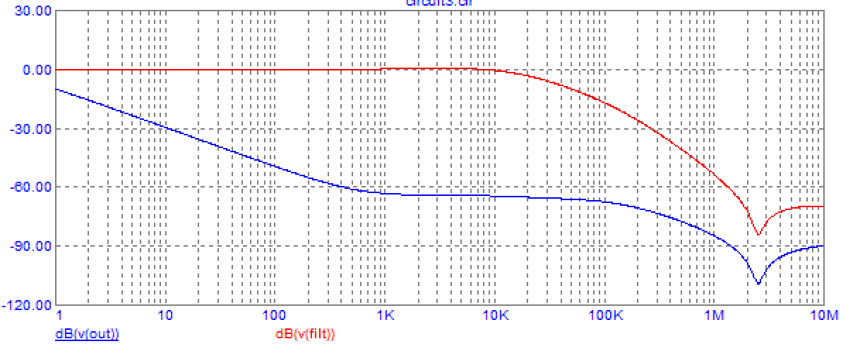
This is the transfer function. It has about 60dB rejection over a wide range of frequencies.

HF rejection will strongly depend on layout. I'd suggest wiring it ghetto style on top of a piece of copper-clad pcb used as ground plane, with the input at one side and the output at the other side. This way, you can't get bitten by a shared impedance in GND between the input and output caps, which would transfer HF input noise into the output...
In the sim, 100µF cap is lowish ESR (1 ohm) and 1µF is MLCC. L1 should be a ferrite bead which can handle required current. Same for Q2, it should handle the current.
EDIT how to design the circuit.
You specified a max current of 0.5A and max voltage 30V. First we need a power transistor for Q2, it should handle the voltage, current, power and safe operating area. With 2-3V dropout at 0.5A it will dissipate less than 2W, so let's use a TO220 or DPAK package.
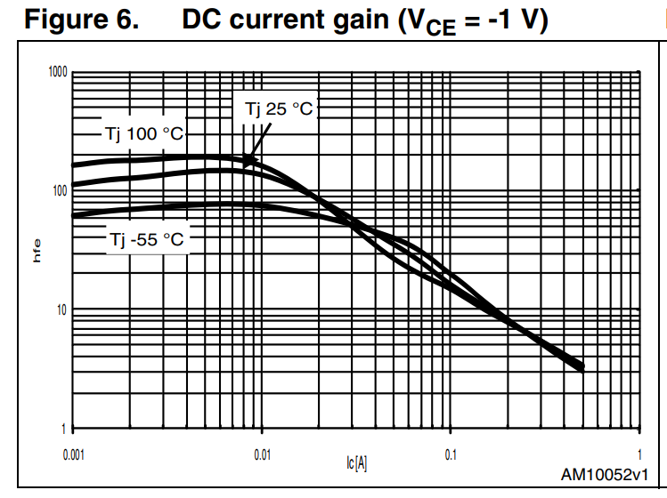
Q1 provides Q2's base current, and Q1 is not a power transistor, so we don't want Q1 to run at more than say 10-20mA for 500mA output, which means Q2 should have at least hFe>25 at 0.5A. The STN9260 you have won't work, as its hFe vs Ic curve shows, at 500mA hFe drops too much.

So let's use TIP127 instead, it's a darlington so it will have plenty of gain, plus I have the Spice model. Datasheet says minimum hFe around 1000, so its base current will be less than 0.5mA. Q1's Ic is S2's Ib plus 2mA from R6. So, Q1's base current will be less than 20µA, which means we can set R2=4k7 for an entirely arbitrary 100mV drop on R2...
Q1's base sees an impedance of C5 in parallel with (R2+D1) ; in this case R1 is irrelevant as D1 is ON, its dynamic impedance will be a few omhs to a few tens of ohms. So at DC R2 dominates the impedance seen by Q2's base.
Q2 Vce is D1's Vf plus Q1 Vbe. If D1 is a red LED, its Vf will be 1.6-1.8V so we get 2.2-2.4V for Q2 Vce, that should work fine. You can use a green LED for an extra 0.2-0.4V.
On power up, C5 will require a few seconds to charge through R2.
In case of short circuit at the output, C5 will discharge through Q1's base into the output. In order to avoid excessive base current, it would be a good idea to add a 100R base resistor to Q1 that I forgot in the above schematic.

