2
\$\begingroup\$

I am designing a 50 ohm 10 watts dummy load for 100-1000MHz frequency range. The signal strength should not exceed -10dBm. The load must be able to dissipate 5 watts minimum, that is +37dBm. The output to the test equipment must be no more than -10dBm. So I need an attenuation of 47dB but to make it easy lets say 50dB.

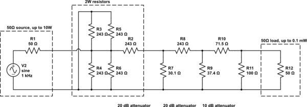
The load consist of two 5W-100ohms resistors. After the load as you can see in the schematic picture there is 3 different attenuators. The first one is 20dB attenuator for 5W dissipation, second one is 20dB-50mW dissipation and the last one is 10dB-50mW dissipation. You can see the values of the resistors on the schematic picture.

Specification for the PCB board:

Trace thickness : 0.036mm

Substrate height : 0.8mm

Trace Width : 1.5mm for 50ohms and 0.3 mm for 100 ohms.

Substrate Dielectric : 4.3

One thing that I couldn't figure out here is the width of the tracks when routing the attenuators as you can see some of them routed with a narrow line. Should it be as thick as 50ohms or something different considering the values, I don't know this because I have never seen it before. Long story short I need help with the circuit and routing the microstrip to have a good impedance match.

enter image description here enter image description here

Looking forward to hear my mistakes and your suggestions about it. Thank you

EDIT

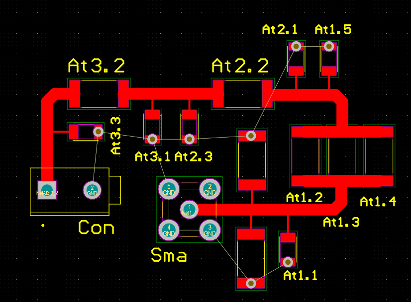
I tried to change the circuit as advised and designed the PCB layout, not sure if its the way to do it.

enter image description here

enter image description here

\$\endgroup\$
4
  • \$\begingroup\$ You need to have a link to the 5 watt resistor's PDF data sheet and identify them on the PCB. \$\endgroup\$
    – Andy aka
    Commented May 26, 2020 at 11:00
  • \$\begingroup\$ I edit the picture and add the link. But I am a college student and because of the current situation of Covid-19 I won't build this project since I don't have access to a lab. So it is going to be a theoretical project. \$\endgroup\$ Commented May 26, 2020 at 11:52
  • \$\begingroup\$ I totally dispute that the so-called power resistors are rated at 5 watts. They are the same physical footprint as 50 mW devices shown elsewhere in your design. \$\endgroup\$
    – Andy aka
    Commented May 26, 2020 at 12:01
  • \$\begingroup\$ Please disregard the footprints as I said I won't build this physically. The matter is the design structure here. \$\endgroup\$ Commented May 26, 2020 at 12:37

1 Answer 1

1
\$\begingroup\$

There are many problems with this design.

First of all, do you really think you can maintain 50 dB of isolation with the two connectors right next to each other like that? Attenuators are generally built in straight lines for a reason, not folded around like that.

Second of all, the design of your pi-network attenuators looks fine, but you can't simply connect a couple of 100 Ω resistors across the input like that. Your resistors "1", "2" and "At1.1" are all in parallel — you need to make sure that the resistance of this parallel combination is 61.11 Ω, which would mean using two 121 Ω resistors or maybe four 243 Ω resistors.

Together, those resistors will be dissipating 80% of the input power, while the entire rest of the attenuator (mainly "At1.2", "At1.3" and "At1.4") will be dissipating only 20% of the input power. You can probably use fewer resistors here.


As far as the trace width goes as well as the overall layout, there's no reason not to combine parallel resistors after the first stage, and you shouldn't use stubs to connect them to the signal path — just merge the pads directly with the trace.

And unless you're trying to use this in the tens of GHz range, the trace lengths are too short to worry much about exact impedances anyway — the parasitics associated with the pads and the components themselves are going to overwhelm any matching issues.


Here's the final design, using E96 resistor values. The theoretical values for 50 Ω attenuators (calculated here) are:

  • 20 dB: 61.11 Ω shunt, 247.5 Ω series
  • 10 dB: 96.25 Ω shunt, 71.15 Ω series

schematic

simulate this circuit – Schematic created using CircuitLab

I would arrange R3-R6 symmetrically around the input connector, keeping the current path loops as short as physically possible. Together, R2-R6 dissipate 99% of the input power, leaving just 100 mW that mostly goes into R7 (whose value is the parallel combination of two 61.11 Ω resistors).

\$\endgroup\$
4
  • \$\begingroup\$ Okay I see my mistakes here with the attenuator part of the circuit and I have to say there wouldn't be a better explanation than yours thank you. But where the 50ohm load will be, I am confused about R1 and R12. And I don't know if it is asking for too much but could you show me how you would put R2-R6 symmetrically like you say? \$\endgroup\$ Commented May 26, 2020 at 13:07
  • \$\begingroup\$ R1 and R12 are not part of the dummy load -- they represent the nominal output impedance of the transmitter and the nominal input impedance of the test equipment, respectively. I'll see if I can add a sample layout to my answer. \$\endgroup\$
    – Dave Tweed
    Commented May 26, 2020 at 14:34
  • \$\begingroup\$ Thanks a lot looking forward to it. \$\endgroup\$ Commented May 26, 2020 at 17:19
  • \$\begingroup\$ I made something myself while waiting .I am pretty sure that is not how you would do it but I'll be glad if you can check it out. \$\endgroup\$ Commented May 27, 2020 at 8:02

Your Answer

By clicking “Post Your Answer”, you agree to our terms of service and acknowledge you have read our privacy policy.

Not the answer you're looking for? Browse other questions tagged or ask your own question.