0
\$\begingroup\$

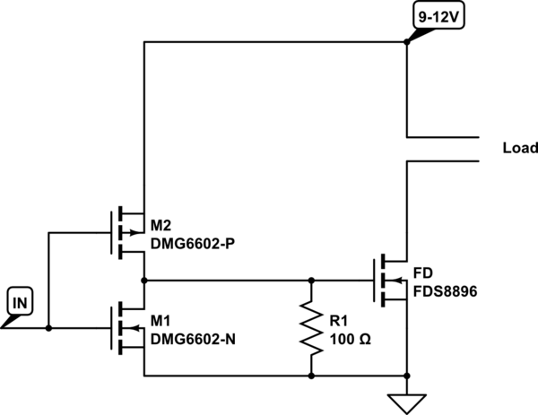
Is there any problem with the below circuit for controlling power supply (as a load switch)?

Switching power supply to load control

Hi, I am using this circuit to switch power supply to a load. I have gone through the datasheets and this looks likes it is okay. But, could someone please confirm if the the circuit used is alright?

The load current does not exceed 10A. The load can be a resistive load or a power supply to another module (not an inductive load).

(I know the MOSFET I used is rated for very high currents). There is no strict requirement on the switching frequency (less than 1Hz) . The supply voltage is 9V-12.6V. The control voltage is 3.3V.

EDIT: [pdf datasheet links]

https://www.diodes.com/assets/Datasheets/DMG6602SVTQ.pdf

https://www.mouser.in/datasheet/2/308/FDD8896_F085-D-1806946.pdf

\$\endgroup\$
10
  • \$\begingroup\$ Whatever you connect to that 2 pin connector (HTR) will always be applied to that R40 resistor, which I assume is your load. In this schematic Q2 would do nothing. I think you meant to connect pin 1 of HTR to your circuit GND. (unless you're using R40 as a shunt?) \$\endgroup\$
    – Stiddily
    Commented Aug 3, 2020 at 12:01
  • 1
    \$\begingroup\$ @Stiddily check again. \$\endgroup\$
    – Andy aka
    Commented Aug 3, 2020 at 12:19
  • \$\begingroup\$ The DMG6602 is not recommended for new designs so why use it? Are you not worried about shoot-thru in the DMG? Add PDF data sheet links please. State what the supply voltages are and the control voltage too. \$\endgroup\$
    – Andy aka
    Commented Aug 3, 2020 at 12:21
  • \$\begingroup\$ @Andyaka I could not find any indication on mouser or digikey, regarding the NRND for this part. If it is NRND, is there any alternative for this? Yes, shoot through is definitely a problem, is there anything you recommend to overcome this ? \$\endgroup\$
    – viru_s
    Commented Aug 3, 2020 at 12:42
  • \$\begingroup\$ Always check with the manufacturer - the mouser data sheet is way out of date. diodes.com/assets/Datasheets/products_inactive_data/… but there is a replacement listed. \$\endgroup\$
    – Andy aka
    Commented Aug 3, 2020 at 12:44

2 Answers 2

0
\$\begingroup\$

The control voltage is 3.3V

The main problem

The gate activation voltage for Q7 is only 3.3 volts!

It will not turn-off the PMOSFET inside Q7 and the circuit will be permanently energized.

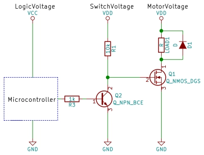
Or, ditch the dual MOSFET device (Q7) and use a BJT in common emitter with a load resistor of circa 1 kohm (aka a level shifter). General idea: -
enter image description here

This can only realistically be overcome with either a control voltage that matches the supply voltage (9 volts to 12.6 volts) or by using an extra input transistor forming a level shifter. This is a show-stopper until fixed. The words below assume it has been fixed.

Given this: -

There is no strict requirement on the switching frequency (less than 1Hz)

Using a level shifter isn't going to be a problem.

The secondary problem

Always check with the manufacturer's website to see if the a device is not recommended for future designs and if so, is an alternative available: -

enter image description here

However, given that this device is probably best replaced with the common emitter level shifter shown earlier, this is moot.

Shoot-through problem

This can be overcome by using a 100 Ω resistor in series with the drains on Q7. The shoot-through current will be limited to a maximum of 12.6 volts ÷ 100 Ω = 126 mA. If that is too much choose a 1 kΩ resistor etc.. The added resistance will slightly slow down turn on or off but, given that you are only switching at 1 Hz and the gate capacitance of Q2 is only circa 3 nF, a response time of less than 5 μs isn't going to be a worry.

But if you fix the main problem using a BJT level shifter, this problem goes away.

Load volt-drop
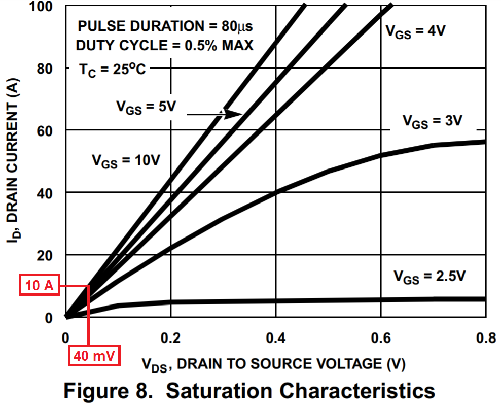
enter image description here

If you can live with Q2's volt-drop of 40 mV when the load takes 10 amps then you're basically good to go. That's a typical value and may be twice this amount across a batch of devices.

MOSFET leakage (\$I_{DSS}\$) into load

When Q2 is off, it might produce typically 1 μA into the load but, again, this is a typical value and it might be as high as 100 μA. If this isn't going to cause activation of some low power circuits in the load then fine.

\$\endgroup\$
3
  • 1
    \$\begingroup\$ Thank you. Considering the above points and given the cost and space, I decided to go with TI's integrated smart high side switch for my use case. \$\endgroup\$
    – viru_s
    Commented Aug 3, 2020 at 20:47
  • \$\begingroup\$ @viru_s OK but it might be a good idea to mention which product you chose for future reference for anyone coming along later - they might be interested in your particular solution. \$\endgroup\$
    – Andy aka
    Commented Aug 3, 2020 at 22:03
  • \$\begingroup\$ I decided to go with TPS2HB16-Q1. :) \$\endgroup\$
    – viru_s
    Commented Aug 13, 2020 at 14:37
0
\$\begingroup\$

Drawing the proper symbols for your dual FET makes it easier to understand:

schematic

simulate this circuit – Schematic created using CircuitLab

When VIN is 3.3V the top PFET (M2) will still have -5..-9V Vgs which means it will be always ON. Also 3.3V is not enough to turn M1 ON. Thus it will not work.

Solution:

If you want fast switching, use an integrated low-side MOSFET driver, like this one. Make sure you double check everything: input logic levels must match your 3V3 signal, min/max supply voltage, etc.

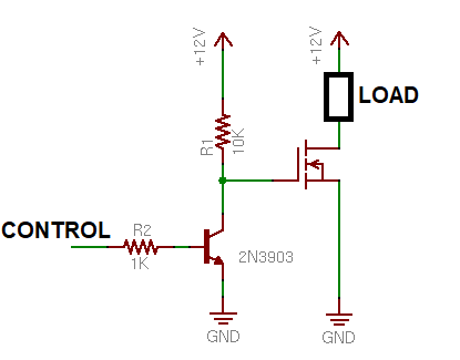
If you don't want fast switching, then any simple schematic with BJTs will do, like this one.

enter image description here

\$\endgroup\$
1
  • 1
    \$\begingroup\$ Thanks @bobflux. I have decided to go with integrated high side switch from TI. \$\endgroup\$
    – viru_s
    Commented Aug 3, 2020 at 20:52

Your Answer

By clicking “Post Your Answer”, you agree to our terms of service and acknowledge you have read our privacy policy.

Not the answer you're looking for? Browse other questions tagged or ask your own question.