1
\$\begingroup\$

I'm trying to build a trans-impedance amplifier shown in the circuit below.

However, with my op-amp of choice, the AD795, I'm a bit confused by their circuit board notes and how to implement them. The input node sends a current in pico-amp range, and the TIA converts it into a voltage at the output. Considering how tiny the input is, it's very critical to maintain the pico-amp resolution at the input. Looking at the datasheet, it shows some notes about this.
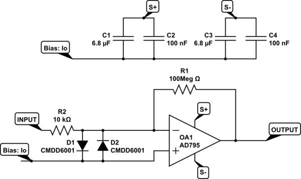
schematic

simulate this circuit – Schematic created using CircuitLab

The first thing they mention is a guard ring in figure 34. Using the unconnected pin pad 1, I can connect it to the bias and draw a guard trace around the input signal path in a no-copper-pour zone so all there is is the signal trace and the guard ring. I can add vias within the ring, as evidenced by what Analog Devices did with this evaluation board for the ADA4350. AD shows the guard being tied to the same potential as the non-inverting node, and that is what I attempted to do. Is this the correct way to form a guard ring, or am I doing it completely wrong?

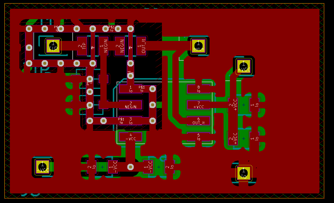
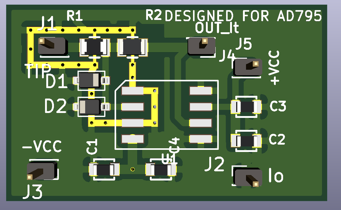
EDIT: Below is my latest attempt at a guard ring, along with the 3D view of it. As you can see, the exposed copper trace is tied to Io, the non-inverting input, while surrounding the inverting input node and the corresponding traces. The ring is also replicated on the bottom plane.

Guard V3 Guard V3 3D view

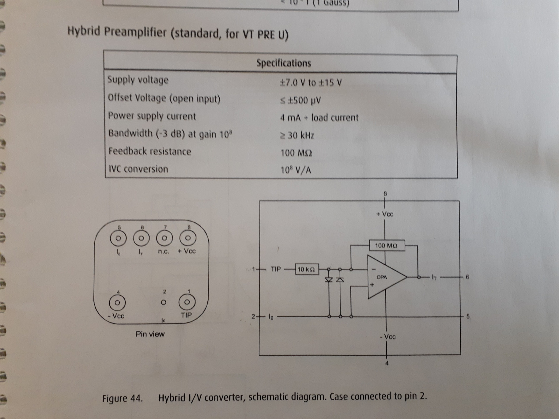
EDIT: Below is my reference circuit for which I'm trying to match up.

Ref Schematic

\$\endgroup\$
2
  • \$\begingroup\$ My reading of the datasheet is that the teflon standoff is an option IF the PCB you are using has too much intrinsic leakage current for the guard trace to work. \$\endgroup\$ Commented Sep 19, 2020 at 3:33
  • \$\begingroup\$ @user1850479 Thanks for your reply. I guess that makes sense. Nevertheless, under what conditions would it be considered too much leakage current? My PCB would only hold the circuit, but what conditions would it require both? In my image, a ground plane is tied to my bias, Io, but would it help if there was no copper pour and I use a guard ring to connect Io for all my components? Also, what kind of Teflon insulated post would be tall enough for an SOIC leg? The standoff option shown in the datasheet seems more for a DIP package than SOIC. \$\endgroup\$ Commented Sep 20, 2020 at 2:42

2 Answers 2

1
+50
\$\begingroup\$

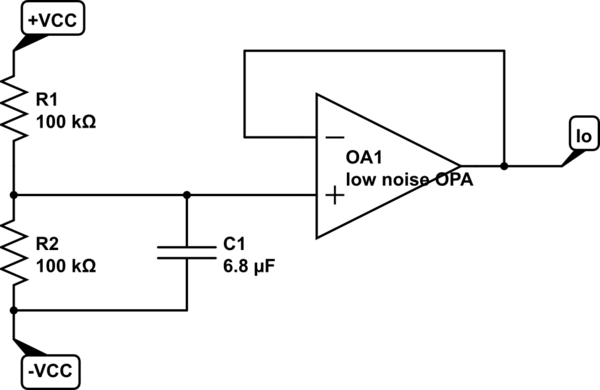
The guard needs to be a low-impedance potential in order to protect what it is surrounding. Using a capacitive-divider like you have is ... not great. To generate a low-impedance mid-scale reference, use a resistor-divider between +VCC and -VCC, and then bypass that with a capacitor to -VCC to filter out noise, and buffer that with a low-noise op amp:

schematic

simulate this circuit – Schematic created using CircuitLab

You can then use this low-impedance Io to drive your guard ring.

A couple more notes about your circuit:

  • You will definitely need a capacitor in parallel with R1 to prevent the AD795 from oscillating. A 1pF cap is a good place to start, but it really depends on a combination of: the feedback resistance (R1 == 100Mohm); the opamp pin input capacitance (2pF); and the capacitance of whatever is connected to INPUT (TIP)
  • If you end up placing the input protection diodes D1 and D2, make sure that they are both low-leakage and low-capacitance. Even though your guard trace surrounds the input node, you'll want to reduce any capacitance between it and the input. Otherwise, you'll hurt your amplifier's frequency response
  • R2 will cause a slight voltage difference between your guard ring and your input (TIP), which could cause current to leak directly from your input to your guard trace. I don't know what source will be driving your input, but if it's anything like a photodiode, you don't need the resistor there and would be better off removing it.
\$\endgroup\$
6
  • \$\begingroup\$ Thanks for replying. This is part of an STM. There' is another external circuit that generates +-VCC with respect to Io, so Io is the ref. voltage to which all other voltages are referenced to, for my TIA. I added a reference schematic that I'm trying to emulate. I went without a cap as the original didn't show one, but I suppose it can't hurt. If the ring has to be tied to a low impedance potential, why does the DS show it tied to the other input? Also, how am I using a capacitive-divider for the guard? Caps are only for power here. \$\endgroup\$ Commented Sep 23, 2020 at 17:30
  • \$\begingroup\$ @BestQualityVacuum Ah, I didn't realize you had an external circuit generating Io, and had assumed that C1-C4 were some kind capacitive divider you were using to create it. The datasheet does indeed show the guard tied to the positive input of the op amp, but it is ALSO connected to the system ground, which is a very low impedance potential. \$\endgroup\$
    – sbell
    Commented Sep 23, 2020 at 18:22
  • \$\begingroup\$ In my case, you can see that my schematic has the non-inverting input tied to Io. Since Io is the reference potential, is what I'm doing correct? Not only did I tie it to the non-inverting terminal, but I used traces to connect to my 'ground plane' which is also tied Io, as you can see by Io's connector at the bottom right. Is there anything that I can improve upon with the way I'm doing it? \$\endgroup\$ Commented Sep 23, 2020 at 18:44
  • \$\begingroup\$ @BestQualityVacuum With your Io being externally generated, yes, the guard ring looks correct. \$\endgroup\$
    – sbell
    Commented Sep 23, 2020 at 19:15
  • \$\begingroup\$ Thank you for your reply. I'm relieved that it looks alright. If you don't mind I have two more technical questions about it. First, does removing the copper fill around and within the ring beneficial, as the way I did with my no-fill zone that encompasses the ring? Second, is the way I'm connecting my ring to the Io copper fill zone (through traces that connect back to the plane) adequate, or would that cause 'ground loops'? Is it better to stick with one path that connects back to the plane? \$\endgroup\$ Commented Sep 23, 2020 at 19:35
0
\$\begingroup\$

I am under the impression that a lot is going wrong in this design...

  1. The guard ring impedance was already mentionned by @sbell. It has to be at the same potential as the signal that you are protecting AND it must be sufficiantly low impedance to catch any current coming from outside the guard ring. The output of your opamp is not at the same voltage syou you need to create it differently. The OPAMP follower (as suggested by @sbell) is a good option.

  2. The way the "connectors" are proposed on this boards are note very conforting. J1 and J2 form the input but they are on opposite sides of the board - what is more is that the power supply is accross the other axis.

    You should put those terminals closer to each other because they are favouring induction loops that do not help you get a good input singal.

    Why not add a BNC connector for the input? You need to be carefull though and choose a connector with low loss.

    You should add another "IO" pin next to the output connector to help avoid an inductance loop there too.

  3. The AD795 does have sufficient drive, but I would add another buffer (OPAMP follower) before it goes off board.

  4. D1 and D2 are both connected to the negative input - there is no need in having the guard ring run under them. Just put them entirely inside the ring.

  5. IMHO there is no need to have the guard ring run under R1. The voltage drop across R1 is negligeable. It might harm more than help.

  6. I wouldn't have a sensitive signal (IO) cover the entire board. By buffering the output signal before having it go of board, the output reference could be shifted to ground so that IO is not loaded by the output pair going off the board.

  7. The input bias current is typically 1pA. I suppose that that does not compare very well to the pA current that you are measuring. There are other OPAMPS that have bias currents that are closer to fA currents.

  8. You may need to load the OPAMP with a resistor to IO or ground. Some OPAMPS do not work well if there is no load - 100k should be enough, at least above 10k to stay within the recommendation of the specification. This may be needed because an unloaded transistor doesn't have optimum operating conditions.

  9. Power supply decoupling does not seem good. Make sure to add one or more capacitors for energy storage, and two other ones for decoupling (with a ration of 1:100 - 1uF/10nF or 100nF/1nF for instance).

  10. Make your input path shorter.

  11. Improve the placement of the decoupling capacitor(s). You could have -VCC or +VCC running under your OPAMP if IO wasn't running accross the board and have a better decoupling path. If you're bringing Gnd to the board, you can decouple to ground and use ground as the reference (when buffering the output using another opamp).

[While I do not consider myself an expert at this, I did design a pH-meter circuit last year coping with the high impedance limitations of it achieving excellent results with low cost components - i.e. the low cost circuit performs at least as well as its predecessors using more pricy OPAMPs with lower input bias].

\$\endgroup\$
3
  • \$\begingroup\$ Thanks for replying. Although I marked @sbell's answer as correct, I appreciate more responses that will help me in my design. Is it fine if the guard surrounds R1 as long as it doesn't go underneath it? Io is a voltage reference, and another op-amp off this board shifts it down to ground, so I don't do it myself. With regards to +-VCC, it's referenced to Io as well. This op-amp circuit is supposed to replace an IVC that had fixed connections, so I can't just add connectors like a BNC. All I can do is add pin headers that will fit. \$\endgroup\$ Commented Sep 23, 2020 at 21:55
  • \$\begingroup\$ The guard ring is there to protect the high impedance signal from receiving disturbing currents. I do not have values, but suppose that your PCB has a 50GOhm conductive path from your 5V supply to your signal, then you would have a current of 100pA disturbing your high impedance signal. The guard ring "shorts" that. The voltage accross your 10k resistor is going to be less than 1uV. With that voltage drop towards the guard ring, even at 1GOhm, the leakage current is well below 1fA. So your 10k is fine inside the guard ring, no need to risk making a short by running the guard ring under it. \$\endgroup\$
    – le_top
    Commented Sep 24, 2020 at 16:01
  • \$\begingroup\$ Even if you IO is coming from another, it may be usefull to filter and buffer it locally. \$\endgroup\$
    – le_top
    Commented Sep 24, 2020 at 16:03

Your Answer

By clicking “Post Your Answer”, you agree to our terms of service and acknowledge you have read our privacy policy.

Not the answer you're looking for? Browse other questions tagged or ask your own question.