1
\$\begingroup\$

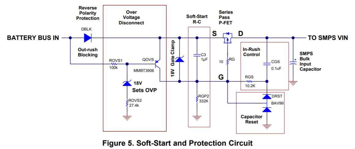
I am reading this App Note. On page 6, Figure 5, they have provided a circuit which helps with the soft start and input protection circuitry.

enter image description here

I am not able to understand the "Capacitor Reset" block on the bottom right. They have mentioned that when there is a power disconnection, the capacitor reset blocks helps to reset the RC time constants of the 1uF and 332k resistor & the 0.1uF and the 10.2K resistor.

I am not able to understand as to how the current or the charge from the capacitor will flow to the ground through those diodes. Can someone help me with the capacitor voltage polarities and the direction of the current flow of those 2 RC sections during that power disconnection?

I have seen diodes placed in parallel to the resistors on microcontroller circuits so that when a power cycle happens, the capacitor is discharged through the diode instead of the resistor so as to provide an indication that there was a power interruption. But I am not able to understand the current flow over here.

Please help to understand.

\$\endgroup\$
2
  • \$\begingroup\$ To see what is going on, you could try to replace the charged capacitor with a voltage source. So now, you should be able to see the capacitor discharging path. \$\endgroup\$
    – G36
    Commented Dec 23, 2020 at 17:13
  • \$\begingroup\$ Sorry, could you explain a little more. \$\endgroup\$
    – user220456
    Commented Dec 23, 2020 at 17:34

3 Answers 3

1
\$\begingroup\$

Definitely, the app note SNVA717 does not discuss a power disconnect condition. Their primary concern is overvoltage disconnect, and most of the document explains the challenges and solution. Let us simulate the Soft-Start and Protection Circuit (Figure 5), part of the Automotive Line Transient Protection Circuit for the case of the Battery Bus disconnect.

I simulate the power disconnect event with a voltage controlled switch OPEN; the voltage source controlling voltage is PULSE(1 0 10m 1u 1u 1000m).

SoftStartAndProtectionwSwitch

The voltages at BatteryBus, at the QIRL source, and VOUT:

batterybusVout

Unlike the power overvoltage condition case, there is no requirement to disconnect SMPS as soon as possible. Capacitor C3 dumps its charge through the series pass PFET QIRL while the latter is in the conducting state (time scale is 30ms, graph I(QIRRL:D) (blue) partly overlaps graph I(C3) (green)).

C3QIRLdraincurrents

After that, node S is dangling because it has no conducting path to ground (graph I(Dblk) (turquoise) overlaps graph Ie(Qovs) (red)).

Snodedangling

DRST11/DRST12 voltages:

diodevoltages

The voltage across DRST11 is V(GDBF) - V(DRSTCP).

DRST11/DRST12 currents:

diodecurrents

At 15ms, the voltage across DRST11 is 50mV, the diode current is a few nanoamperes. At 24ms, the voltage across DRST12 is 385mV, the diode current is 7.8μA, at 30ms, 4.7μA, at 100ms, 450nA.

As you see, the DRST11/DSRST12 currents drop to infinitesimal values early, and capacitor C3 remains charged indefinitely long, because node S is dangling, and the current path is not closed. The DRST block cannot fix it, and there is no need to worry.

\$\endgroup\$
2
  • \$\begingroup\$ Thank you for the answer. But in this - youtube.com/watch?v=Vq6cxmzRnyw&t=326s video the person says that the two RC sections are used to reset. I am not able to understand. \$\endgroup\$
    – user220456
    Commented Dec 24, 2020 at 16:17
  • \$\begingroup\$ +1 for graphs on a white background with fat lines. That is so much easier to read. \$\endgroup\$ Commented Mar 19, 2021 at 11:56
0
\$\begingroup\$

As you already suggested, the diodes are probably providing a lower ohmic path for discharging both capacitors.

As far as I understand it works as follows:

Consider the following:

  1. Once the battery is disconnected and the input voltage falls below 18V + 2 diode voltages, the reverse polarity and overvoltage disconnect block no longer do anything. At this point, the capacitor \$C_3\$ is charged to approx. 18V.
  2. The two diodes are in parallel to the resistors \$RGS\$ and \$RGP2\$, thus offering an unidirectional lower ohmic path
  3. Since the SMPS acts as a power converter, it will drain the input power (in this case the power from both capacitors) until either its undevoltage lockout kicks in, or the PFET's \$V_{GS}\$ (or voltage across \$C_3\$) becomes so small, thus turning the PFET off.

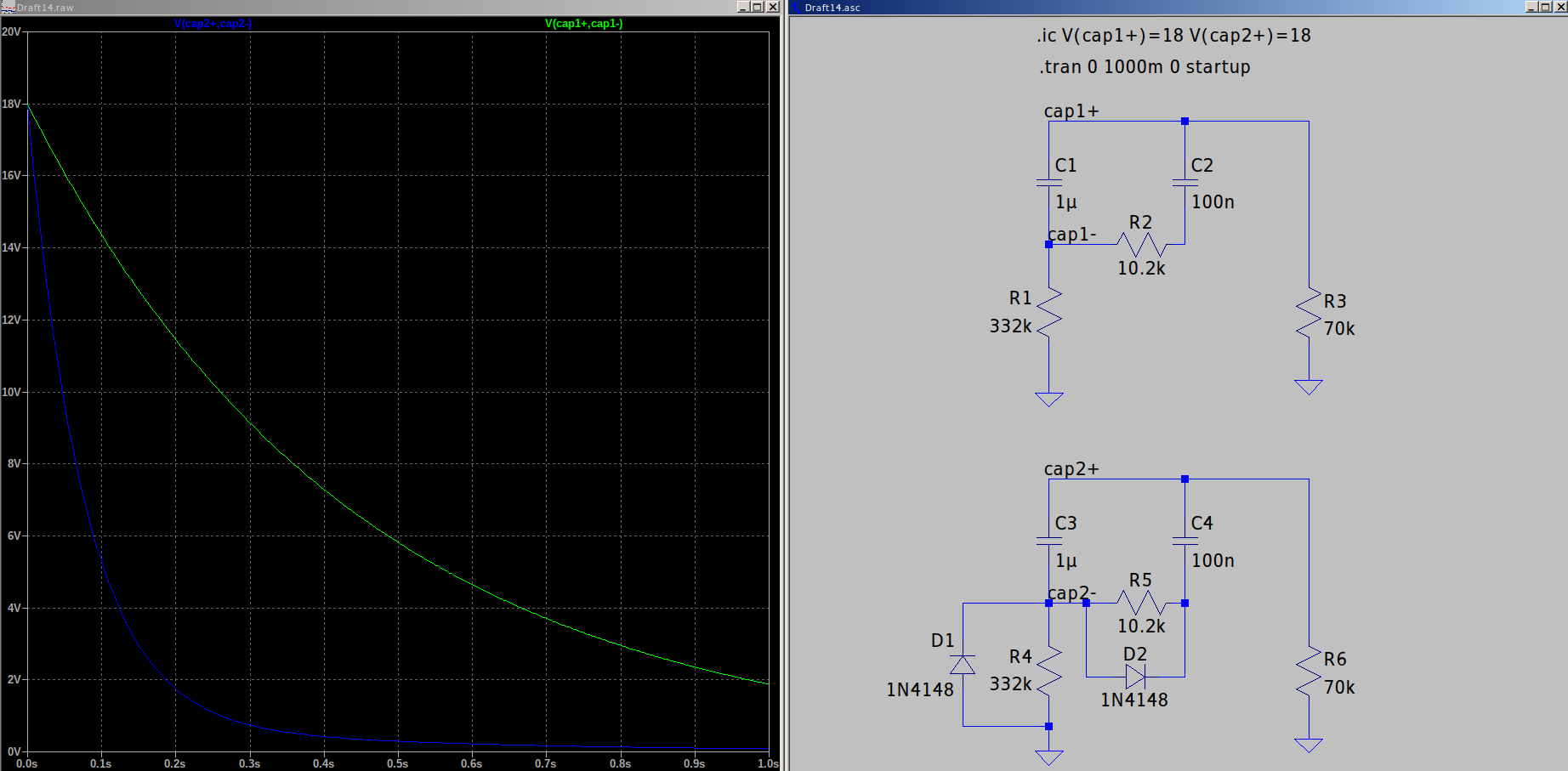
If you disconsider the PFET for the moment and replaces the constant power load with a resistor, you could run a quick simulation comparing both discharging times:

circuit_1

\$\endgroup\$
2
  • \$\begingroup\$ Thank you for the answer. Could you please provide the direction of the current during the diode conduction? \$\endgroup\$
    – user220456
    Commented Dec 25, 2020 at 12:45
  • \$\begingroup\$ Current in a diode flows from anode to cathode. \$\endgroup\$
    – vtolentino
    Commented Dec 25, 2020 at 16:17
0
\$\begingroup\$

The working of Over Voltage Disconnect block during an over-voltage condition is already explained in the application notes as:

  • The component ROVS1, QOVS and the zener diode set the OVP voltage level at the circuit input.

  • Initially when the input voltage is below 18 V, the QOVS transistor will be in an off state allowing the capacitor C3 to be charged through C3 and RGP2 thus turning on the PFET.

  • Once the input voltage reaches approximately 18V plus 2 diode drops, the transistor QOVS will be turned on since the base of QOVSis held at the zener voltage of 18 V. When this transistor is turned on, it discharges capacitor C3 and pulls the gate of PFET to its source and thus turning the PFET OFF.

  • Once the input voltage goes back below 18V, the OVP condition is cleared and QOVS is again turned off. This allows the capacitor C3 to be slowly charged again, resulting a soft-start at the output.

Now regarding the remaining blocks, the working is same in both OV-Disconnect and Input disconnect since essentially, the both are doing same (disconnect the supply from Batetry Bus).

  • The capacitor C3 continues to supply power to the SMPS Vin. While supplying power, C3 has two parallel paths to conduct current:
    1. Through R_GP2.
    2. Through Capacitor-reset Diode D2 (say), through which it can discharge faster into (load connected to) SMPS Vin.
  • Similarly C_GS has two paths to discharge:
    1. Through R_GP2 + R_GS
    2. Through Capacitor-reset Diodes D1 + D2.

The purpose as I see is to finally dissipate the capacitor energy into load connected to SMPS VIN pin, and the Capacitor-reset diodes are catalysing the discharge process.

\$\endgroup\$
1
  • \$\begingroup\$ Thank you for the answer. Could you please mention the voltage polarity and the current directions in a separate image along with your answer (during the input disconnect and overvoltage condition) ? \$\endgroup\$
    – user220456
    Commented Apr 4, 2021 at 16:58

Your Answer

By clicking “Post Your Answer”, you agree to our terms of service and acknowledge you have read our privacy policy.