1
\$\begingroup\$

I am really new to electronics and BJT. I would like to know why is the input characteristic curve of common collector configuration [Ib-Vbc] is different from other 2 input characteristic curves. What actually accounts for this difference?

update:

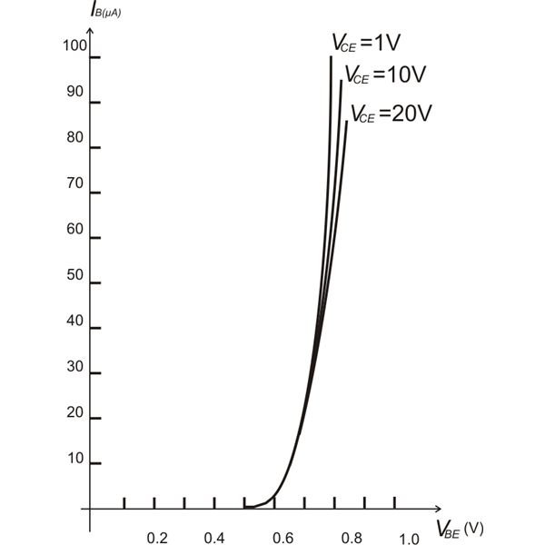
@jippie the input characteristic curve of common emitter configuration is as follows:

enter image description here

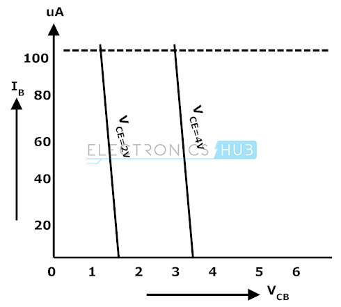
but the input characteristic curve for a common collector configuration is :

enter image description here

can I know what actually causes this difference?

\$\endgroup\$
1
  • \$\begingroup\$ Can you give a couple example graphs of the curves you refer to? \$\endgroup\$
    – jippie
    Commented Jun 6, 2015 at 11:14

2 Answers 2

1
\$\begingroup\$

Kathi, it helps to realize that the signal voltage Vbc (between base and collector) is identical to the signal voltage Vbo (between base and common ground). This is because the internal ac resistance of the DC voltage source (connected to C) can be regarded as zero.

Secondly, in common-collector configuration there is a emitter resitor Re between the emitter node and ground. Hence, the input characteristics of this configuration contains the base-emitter path in series with the resistor Re.

In this context, it is important to realize that the current through Re is beta times larger than the current into the base node. Hence, the voltage drop across this resistor - resulting from the input signal at the base - is correspondingly larger.

This is the well known feedback effect which determines the whole input characteristics. As a result, the input resistance of the whole circuit is r(in)=rbe + beta*Re. (If the current through Re would be identical to the base current Ib the input resitance would be only rbe+Re)

\$\endgroup\$
4
  • \$\begingroup\$ Both graphs clearly show the 0.6V base-emitter voltage drop, which only applies when you consider the DC model. Can you elaborate how the small signal AC model applies here? \$\endgroup\$
    – jippie
    Commented Jun 7, 2015 at 19:16
  • \$\begingroup\$ Sorry - in the 2nd graph I cannot see any 0.6 V voltage drop, can you? \$\endgroup\$
    – LvW
    Commented Jun 7, 2015 at 21:30
  • \$\begingroup\$ I think so: The the line V(CE) = 2V, starts for I(B) = 0 at approximately V(CB) = 1.5V. That leaves approximately half a volt for V(BE). \$\endgroup\$
    – jippie
    Commented Jun 8, 2015 at 5:54
  • \$\begingroup\$ And what is the importance of this "information"? Any surprise? \$\endgroup\$
    – LvW
    Commented Jun 8, 2015 at 6:13
0
\$\begingroup\$

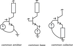
Below is the large signal circuit diagram for common emitter, base, and collector configuration just for clarity of visualization.
enter image description here

The voltage source is where the input voltage is applied and the arrow pointer indicates on what port and in what direction the input current is measured.

But, there is a catch, the plotted graphs use different reference terminal. The horizontal axis of your first graph referenced the input voltage at the base to the emitter, therefore, higher base to emitter voltage does indeed increase the base current because the Base-Emitter junction will be more forward-biased, therefore there is an increase in the diffusion emitter current, and therefore there is also an increase in the recombination base current. It is basically a diode equation curve.

Now, for your second graph, the horizontal axis is instead the collector voltage referred to the base. Because we know the collector is at a fixed supply voltage (look at the diagram), increasing the collector to base voltage is, in reality, decreasing the base voltage referred to ground. Based on the same reasoning as before, decreasing the base voltage results in a decrease in base current. So the curve is basically the first curve, but flipped horizontally and then offset to the right by VCE (which is equal to the supply voltage). Remember, VCB = -VBE + VCE.

How about the common base? The graph you have seen will most likely be a graph with a horizontal axis of base voltage referred to the emitter voltage. Therefore, an increase to the base-emitter voltage, again, results in an increase in the emitter current (look at the graph, the input current is now the emitter current). So it will look basically the same as the first graph, but scaled by a factor of 1/(1-alpha).
\$\endgroup\$

Your Answer

By clicking “Post Your Answer”, you agree to our terms of service and acknowledge you have read our privacy policy.

Not the answer you're looking for? Browse other questions tagged or ask your own question.