0
\$\begingroup\$

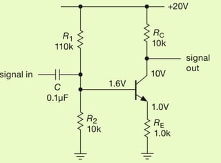
I am not an electrical engineer but I was just reading the book - The art of electronics. I am just a bit confused about how to analyze this amplifier circuit.

In this case, why are R1 and R2 in parallel?

I would think it makes more sense for R1 and Rc to be in parallel. Even if that is not the case, when we look into the circuit, shouldn’t there also be a large impedance due to the gain of the transistor? Thanks in advance.

transistor circuit

equation

\$\endgroup\$
3
  • 1
    \$\begingroup\$ What book were you reading when you found this? Didn't it provide any explanation for the circuit or the equation? \$\endgroup\$ Commented Apr 19, 2021 at 20:32
  • 1
    \$\begingroup\$ Which book? To me it looks like that picture is from The Art of Electronics book, anyway given without attribution. Though any book might have very similar picture with description, it's so common. \$\endgroup\$
    – Justme
    Commented Apr 19, 2021 at 20:35
  • \$\begingroup\$ Sorry, first time here but good eye! It is from the art of electronics. I will edit the post. Thanks for pointing it out \$\endgroup\$ Commented Apr 20, 2021 at 1:38

2 Answers 2

2
\$\begingroup\$

why are R1 and R2 in parallel?

R1 and R2 are not in parallel. However, the impedance provided by R1 and R2 to the input is found by the parallel resistance formula. This is because the power supply has a much lower impedance than either R1 or R2. So, in calculating the input impedance, we treat the (positive) power rail as if it were ground. Then, in our imaginary world where the (positive) power rail is ground, R1 and R2 do become parallel.

shouldn’t there also be a large impedance due to the gain of the transistor?

Yes, there is. But the author(s) chose to ignore that detail in this particular case. The impedance provided by the path through the base would also be in parallel with the impedances of R1 and R2. In this case, it is probably just as significant as the impedance of R1. However, R2 is more significant that either R1 or the impedance through the base.

\$\endgroup\$
0
\$\begingroup\$

\$R1\$ and \$R2\$ form a voltage divider, that 'looks' like a single resistance to a voltage at the sum point. This is called a Thevenin equivalent, from Thevenin's theorem that tells us that any set of voltages feeding resistors to a summed point can be reduced to a single source voltage connected via a single resistance. More here: https://www.electronics-tutorials.ws/dccircuits/dcp_7.html

The circuit shown is a first-order high-pass filter. The equation they're giving, \$ C \ge \frac {1} {2\pi f (R1 \parallel R2)}\$, is how to choose a coupling capacitor so the -3dB cutoff frequency cutoff frequency, commonly expressed as \$f_c\$, is above some chosen frequency \$f\$.

This -3dB cut-off point happens when cap \$C\$ impedance is equal to the Thevenin equivalent for \$R1\$ in parallel with \$R2\$. Make the cap bigger, the -3dB point shifts lower; make the cap smaller, it shifts higher.

What is \$f_c\$ for this filter? We can estimate it from the values given:

  • \$f_c = \frac {1} {2 \pi (R1 \parallel R2) C} \$

or about 174 Hz.

Now what's going on at the transistor base? A little bit of current flows into it. But since the emitter follows the base because of \$R_E\$, the AC component of the current is small and thus doesn't contribute much to the Thevenin sum.

Nevertheless, the path to the base and \$R_e\$ does shift the -3db \$f_c\$ up a bit, and a deeper analysis of the design would account for it.

\$\endgroup\$
1
  • 2
    \$\begingroup\$ At the -3dB frequency the voltage gain will be down to 70.7% (not 50%) of midband gain. -3dB = 20log(0.707). This is the half power frequency. \$\endgroup\$
    – user173271
    Commented Apr 19, 2021 at 22:32

Not the answer you're looking for? Browse other questions tagged or ask your own question.