Page 4 only indicates the Thermal resistance from junction to Solder Pads.
Electrical thermal resistance { junction/solder point} with efficiency % \$ η_e=47,~R_{th JS} = 4.2 ~'K / W\$
But that means all 3 solder pads.
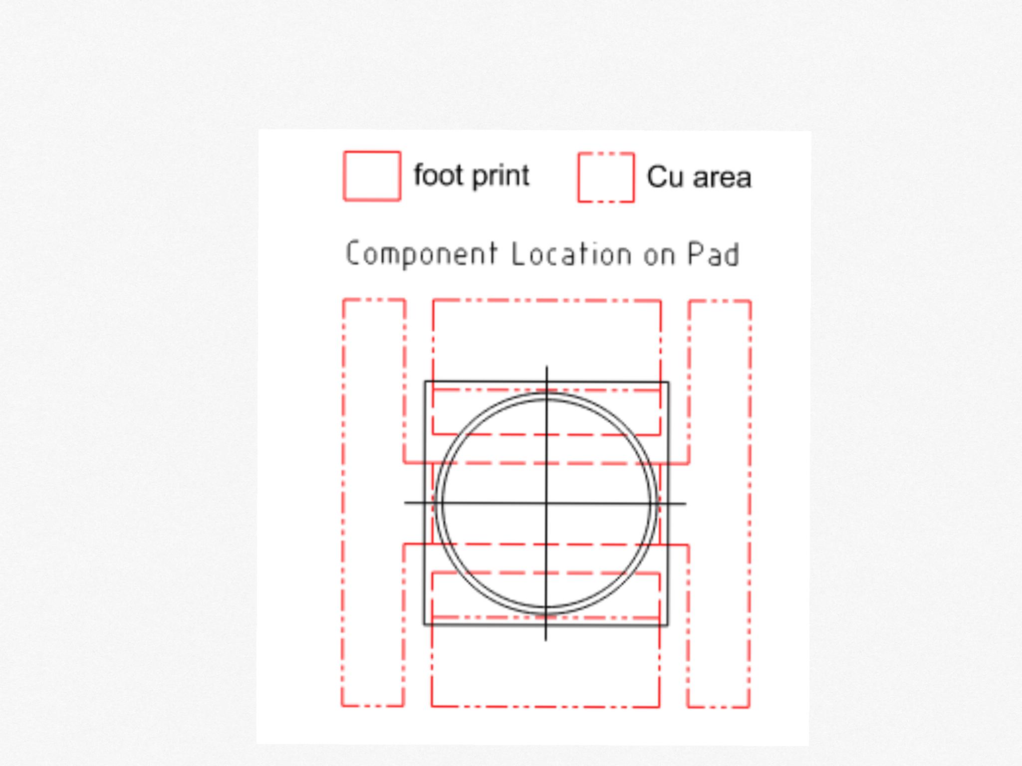
I anticipate the size of the middle pad over MCPCB can be shrunk considering improvement of MCPCB for the middle solder point to ambient has better conduction to the substrate. Ultimately you want to spread the heat as much as possible to reduce thermal hot spot of the junction as the total thermal resistance Rja=Rjs+Rsa.
It should to be verified somehow to understand what you are compromising by reducing the heat pad size.
Edit 1
Without specs for Pd and Tmax rise,and total watts per square area and type of air flow , one cannot assume eliminating the middle pad wings will have any detrimental effect.
I suspect it helps, but if you perform a test to verify this assumption, then you may confirm this.
The ceramic thermal conduction to Al might be 5 to 10 x better than air but the area of copper pads is also proportional to the heat transfer.
Consider 3 scenarios and decide which is best.
- No wings on centre thermal pad.
- With wings on centre pad
- Copper pour to all LEDs to centre pad.

- estimate Area of 3 pads only = 10 units and each wing 3 units so thermal conduction is improved by 16/10 or 60% to Al substrate. This assumes critical path for Thermal conduction to substrate is 5 to 10 times better than from substrate to air.
- Copper pour to middle pad would be best.


