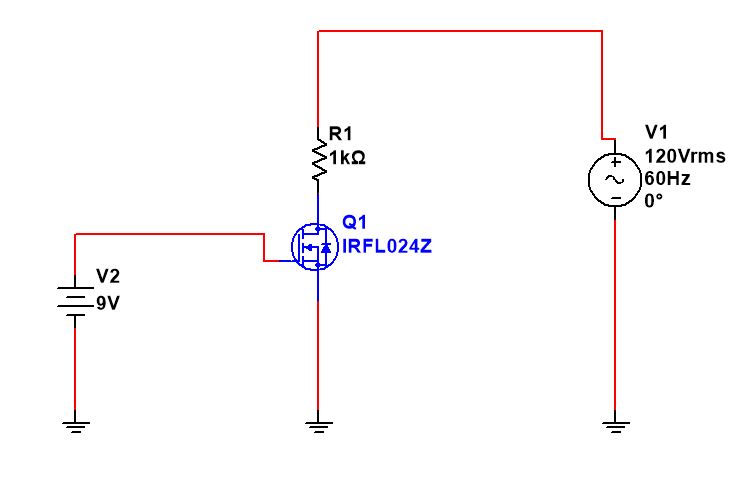
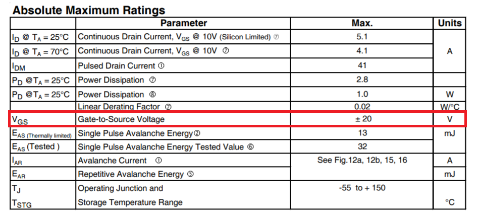
My application is such that the current needs to be blocked or allowed in the positive half cycle using the gate triggering as shown. But in reverse voltage cycle it must pass through the load. I can understand, in the reverse mode even if the gate is NOT triggered, the body diode will allow to flow the current through the load which meets my criteria, but in that case when negative peaks occur, a voltage of -111v will be applied to the GS junction which is pretty high. As we know typically maximum GS voltage is around 20V, but how about in the reverse GS situation? is there a parameter like "reverse gate-source voltage"? if yes, what can be the average value for this parameter?
-
\$\begingroup\$ You must clamp Vgs to < absolute max -20V with high Gate R in series and not use Rd=1k which will go up in smoke when not rated for V or Pd. \$\endgroup\$– D.A.S.Commented Aug 8, 2021 at 12:18
-
3\$\begingroup\$ I don't understand the question. In your diagram, Vgs is +9V or 0V, period. The source is connected to 0V, so how could anything reach -111 V? 120 Vrms is 170 Vpeak anyway, but most of that appears across the load in any case. When the MOSFET is off, the drain will reach +170 V, but the body diode will clamp it to about -1 V on the negative half cycle. \$\endgroup\$– Dave TweedCommented Aug 8, 2021 at 12:25
-
\$\begingroup\$ Q1 source is on bottom, Drain on top. \$\endgroup\$– rdtscCommented Aug 8, 2021 at 15:38
-
\$\begingroup\$ I have seen the error, will rectify it shortly \$\endgroup\$– SayanCommented Aug 8, 2021 at 16:30
1 Answer
As we know typically maximum GS voltage is around 20V, but how about in the reverse GS situation? is there a parameter like "reverse gate-source voltage"?
Can you see the +/- symbol next to "20"? The maximum reverse gate source voltage is 20 volts and is the same as the normal gate source voltage.
but in that case when negative peaks occur, a voltage of -111v will be applied to the GS junction which is pretty high.
The schematic you have shown will not permit that voltage because the gate source voltage is fixed at +9 volts by V2.


