0
\$\begingroup\$

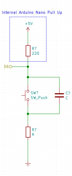
The D6 is a digital pin (input) of the Arduino Nano.

Function of the circuit: If the button is not pressed the internal pull up pulls the input D6 up to 5 V (high). If the button is pressed the input D6 is low (0 V). The capacitor and resistor are used for debouncing the button.

My Question: Is the wiring concept of the capacitor and resistor a low pass? And can I calculate the capacitor with $$f=\frac{1}{2\pi R C}$$?

circuit

\$\endgroup\$
9
  • \$\begingroup\$ The simplest RC lowpass filter is a resistor in series and a cap to ground and that's it. So no, this schematic isn't a low pass filter, the cap should go to ground and you should place the filter between the switch and the MCU, since I'm guessing the purpose is hardware debouncing. \$\endgroup\$
    – Lundin
    Commented Nov 5, 2021 at 11:49
  • \$\begingroup\$ The purpose is to debounce the button \$\endgroup\$
    – Less
    Commented Nov 5, 2021 at 11:57
  • \$\begingroup\$ But when the button ist pressed....there is a signal flow from ground to D6. That's why I drew the circuit so that the resistor is in front of the capacitor. \$\endgroup\$
    – Less
    Commented Nov 5, 2021 at 12:01
  • \$\begingroup\$ The standard solution would be ground -> switch -> series resistor 1k -> pull down cap 100nF -> MCU input. The more professional solution would be to connect a bench supply to the raw unconnected switch, measure the contact bounce with a scope, determine a reasonable cut-off frequency, then calculate some suitable R and C. \$\endgroup\$
    – Lundin
    Commented Nov 5, 2021 at 12:03
  • 2
    \$\begingroup\$ @Lundin: A contact bounce can never be a pure sine wave. At the most parasitic level it is a bunch of RLC circuits (charging parasitic L and C) which creates a complicated circuit with many resonances. Those freqs are triggered a step in current (the switch) with infinite harmonics. The parasitics make the ringing (sine waves) not the contact bounce. The purpose of the capacitor the OP is asking about is to over dominate those C parasitics, removing the harmonics that trigger ringing. If the charging current were limited then at best you would have a sawtooth due to C*dv/dt not a sine wave. \$\endgroup\$
    – Jay M
    Commented Nov 5, 2021 at 16:19

2 Answers 2

2
\$\begingroup\$

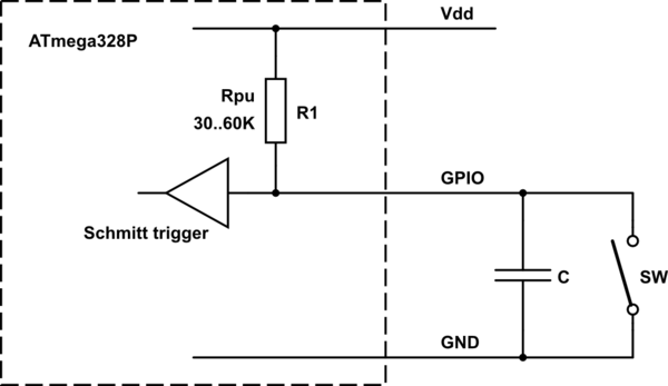
You can just connect a capacitor from I/O pin D6 to GND and connect the switch in parallel with it.
schematic

simulate this circuit – Schematic created using CircuitLab

The Arduino Nano uses the ATmega328P which has Schmitt trigger inputs for all its GPIO pins. This ensures that the relatively slow rise voltage on the capacitor will not cause input 'chatter' as it passes through the uncertainty voltage range found in logic signals.

When the switch is pressed, it will short-circuit the capacitor, drawing an instantaneously-large discharge current through itself. This arrangement of switch and debounce capacitor is very common and has been used in millions of products and equipment around us for decades. Few or none of these switches or capacitors have been damaged by this.

You need to know the switch bounce period. You should take this from the datasheet. If you do not have this, most switches are 3..10 ms so you can use a working guess value of 10..20 ms. But look the value up if at all possible.

To calculate C, you need the following values:

  • Switch debounce period (or use 15 ms) tdb
  • Schmitt input trigger voltage (min.) Vtmin
  • Pull-up resistor value (min.) Rpumin
  • Supply rail voltage (min.) Vddmin

Note that the minimums are used. The maximum for any of these values will make the RC charging or detection time longer, which means the circuit will debounce its input for longer. If it debounced for a shorter time when the RC tolerances changed, the switch might still be bouncing and those might get detected, so this goes in the safe direction.

Some of these can be found in the ATmega328P datasheet:

  • Vt = approx. 2.6 V (from Pin Threshold graph)
  • Rpu = 30..60 kohm, so Rpumin = 30000 ohms

For the Arduino Nano supply rail, I'll assume (a terrible word) a 5 V +/- 0.25 V regulator. So Vddmin = 4.75 V.

Transposing the capacitor charging equation $$v=V(1-e^\frac{-t}{RC})$$

for C gives $$C=\frac{-t}{R*ln(1-\frac{v}{V})}$$

So $$C=\frac{-0.15}{30000*ln(1-\frac{2.6}{4.75})}=630 nF$$

Use 680 nF.

\$\endgroup\$
1
1
\$\begingroup\$

schematic

simulate this circuit – Schematic created using CircuitLab

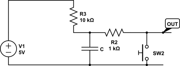
This is more correct, no internal pull-ups.

R2 limits the current through the switch. \$I_{SW}=\dfrac{5V}{1000\Omega}= 5mA\$. The \$\tau_c=R_3C=10k\cdot C\$ for charging the capacitor, while it is being discharged with \$\tau_d=(R_3 \parallel R_2) C\$. The remaining capacitor voltage is \$V_c=5V\dfrac{R_2}{R_2+R_3}=0.45V\$

\$\endgroup\$
1
  • 3
    \$\begingroup\$ Why is avoiding internal pull-ups valuable? They're there to be used, to save part count and simplify circuits, if their characteristics are suitable which they certainly are here. And where is 'correct' defined and how is using more parts wastefully more 'correct? \$\endgroup\$
    – TonyM
    Commented Nov 5, 2021 at 11:24

Your Answer

By clicking “Post Your Answer”, you agree to our terms of service and acknowledge you have read our privacy policy.

Not the answer you're looking for? Browse other questions tagged or ask your own question.