1
\$\begingroup\$

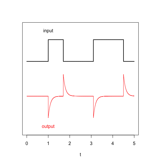
I have a circuit whose input is either at the supply voltage or ground. This feeds into a high pass filter with a time constant around \$RC \approx 1\ \text{s}\$. Example input looks like the black line below, while example output is like the red line. In this case the output is inverted, but this is not really important.

Example input and output

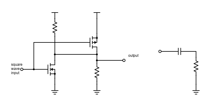
The signal source has high output impedance, so I have come up with the MOSFET circuit below (left fragment) which always has a low impedance path to the rail (ground if input is high, supply if input is low). The idea is that the left side of the capacitor will always follow the input signal (only inverted), giving essentially zero output impedance and not loading the RC filter as seen in the right fragment.

circuit diagram

My questions are:

  • Will this circuit work as intended?
  • Is there a name for this simple configuration?
  • Is there a better way of doing it?
\$\endgroup\$
3
  • \$\begingroup\$ If the input is high, both FETs will be on and short the supply. Why not use a logic gate as a buffer? \$\endgroup\$
    – bobflux
    Commented Jul 14, 2022 at 7:01
  • \$\begingroup\$ Double check if you intended to use depletion mode mosfets in your schematic. You really need enhancement mode mosfets for this application. Also double check if you id not swap the source and gate \$\endgroup\$
    – Ferrybig
    Commented Jul 14, 2022 at 7:59
  • \$\begingroup\$ I always get confused about MOSFET symbols. I think I have corrected it with enhancement mode now. The left one should be npn and the right one pnp. \$\endgroup\$ Commented Jul 15, 2022 at 1:45

1 Answer 1

5
\$\begingroup\$

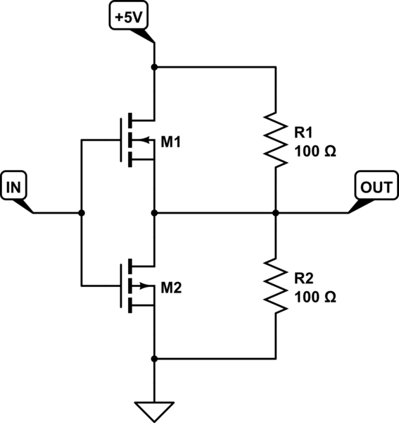
What you've drawn is essentially this:
schematic

simulate this circuit – Schematic created using CircuitLab

I think you have tried to combine a pair of common-source (drain?) MOSFETS to obtain some kind of push-pull stage. That's not a bad idea, but it's badly implemented here.

For starters, M2, a P-channel device is upside down. In this configuration its gate will have to be very negative (way lower than its source, which is at ground potential, 0V) to switch on. Since that never happens, the MOSFET M2 is always off.

Secondly, M1 is configured is common-drain, also known as "source follower". That's OK, in that its source follows gate potential, but it's going to fail in this application because the source is always a couple of volts lower than the gate, not exactly the same.

Lastly, those resistors do play a role when paired with a single common-drain or common-source transistor, but in a push-pull setup they are redundant. The idea is to replace the resistor with another transistor, not supplement it.

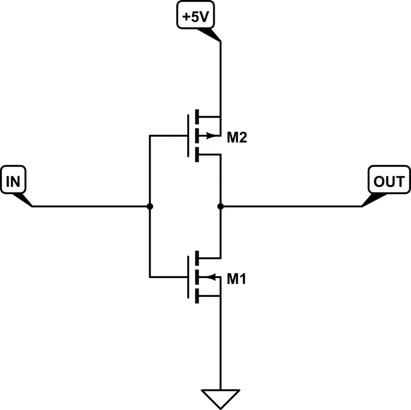
Since your input signal is square (digital), and you want a lower impedance copy of it, common-drain arrangements are not very useful here. Perhaps a better solution would be a pair of common-source MOSFETS in a totem-pole configuration. In this way, each transistor is either fully on or fully off, in keeping with the digital nature of the source:
schematic

simulate this circuit

Without more information regarding frequency, amplitude, rise/fall times and so on, it's impossible to know if this simple solution will work for you, or even what power supply voltage is required. This particular approach suffers from shoot-through, a condition where during the rise and fall of gate potential, there may be a period of time during which both transistors are conducting, resulting in a potentially large current being drawn from the supply voltage source.

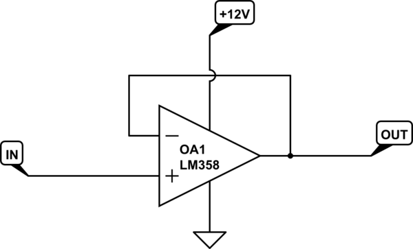
Is there any reason why you can't use an op-amp as a voltage follower, to provide a low-impedance copy of the input? It's dead simple:
schematic

simulate this circuit

This solution provides an output impedance very close to zero, although it will be current limited to about 10mA or so. The output will be an almost identical copy of the input, and presents almost no load at all to the input source. Also, it's quite insensitive to power supply voltage, what goes in, comes out. Beware of op-amp limitations such as output voltage range (which always depends on its two power supply potentials).

\$\endgroup\$
2
  • \$\begingroup\$ I've fixed the polarities and enhancement vs. depletion model in my circuit diagram. The "totem pole" is much cleaner than my original configuration and looks like it should work for me. I really only care about sinking/sourcing current during transitions, and it looks like the totem pole will go to zero current once the capacitor is charged. I just need to figure out how to deal with the "shoot through". The reason I didn't consider an op-amp is because I need to sink/source at least 100 mA and I wasn't sure if I could easily find an op-amp that could handle that much current. \$\endgroup\$ Commented Jul 15, 2022 at 2:12
  • \$\begingroup\$ If you don't need the output to be rail-to-rail, you can use an NPN (top) and PNP (bottom) pair with emitters and bases tied together. There is little chance for shoot-through, and 100 mA is no problem for devices like 2N3904 and 2N3906. \$\endgroup\$
    – PStechPaul
    Commented Jul 15, 2022 at 3:37

Your Answer

By clicking “Post Your Answer”, you agree to our terms of service and acknowledge you have read our privacy policy.

Not the answer you're looking for? Browse other questions tagged or ask your own question.