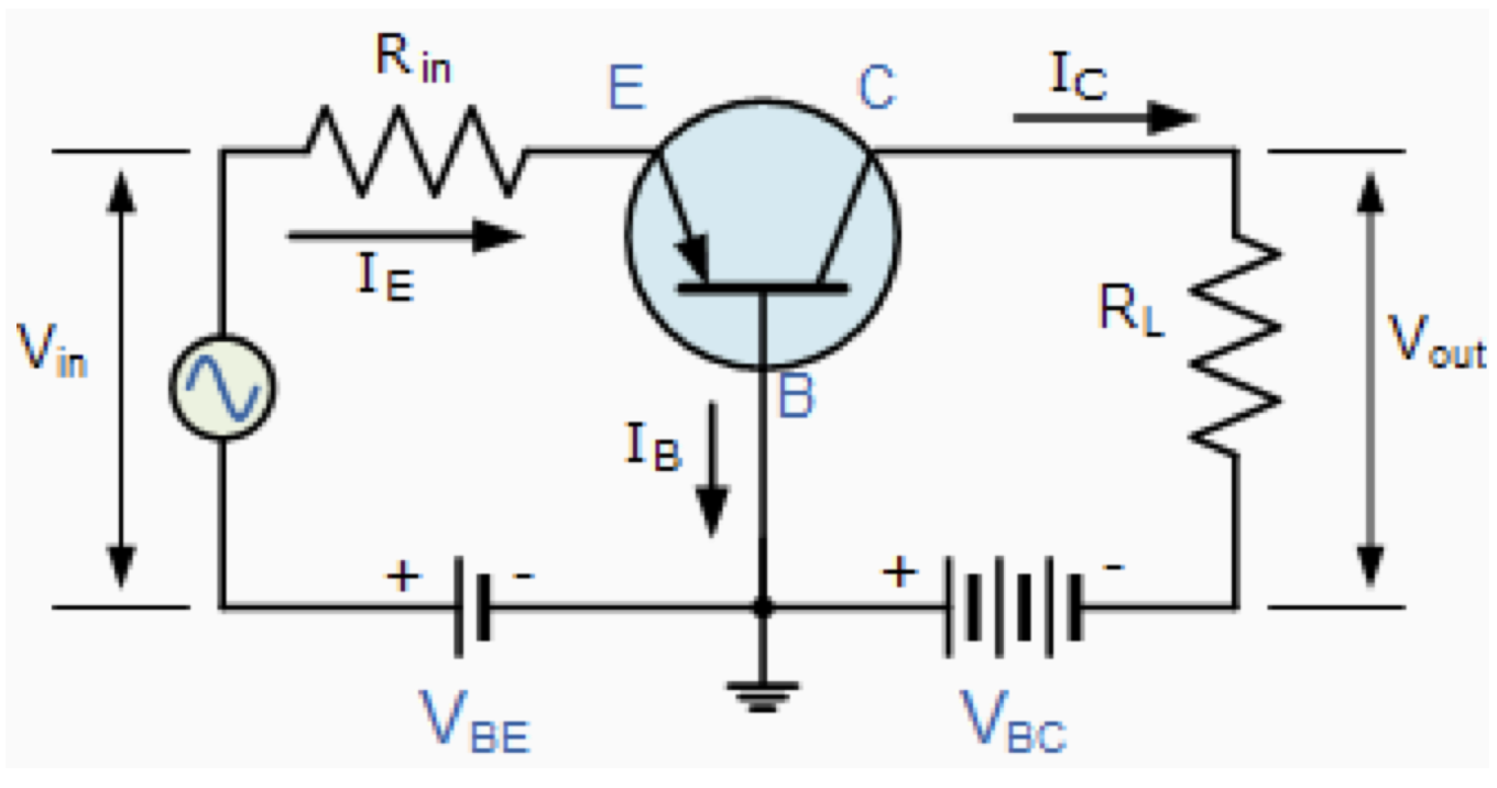
In the circuit given below, how can I apply KVL to the loop on the right side? The reference node being connected to the positive terminal seems wrong.
-
1\$\begingroup\$ If you moved the ground symbol to the bottom right corner would it look right? It doesn't make any difference to how you solve it. We're just more used to thinking of ground as being the most negative point on a circuit but it doesn't have to be. \$\endgroup\$– TransistorCommented Sep 18, 2022 at 16:03
-
\$\begingroup\$ There is nothing magic about the point marked with the Ground symbol - that symbol just marks the spot we want to call "Zero volts". In most circuits, particularly in the demonstration circuit you show, it does not indicate any connection to the outside world. \$\endgroup\$– Peter BennettCommented Sep 18, 2022 at 23:47
3 Answers
Direct answer
I'll write more, later. But first....
There's nothing specifically wrong about connecting the positive terminal of a DC voltage supply (battery or mains-powered) to a 'ground'. A ground reference is just a way of saying, "This node is to be treated as the 0-reference point for the rest of what I'll be talking about."
Nature itself doesn't care at all about the idea. It doesn't know about it. Nature will just do whatever it does, anyway. The ground-mark is just a convenience for us humans. That's all it is. It changes nothing about the circuit, itself.
So get that right!
This means you can move the ground reference to any node you want without changing the schematic's function.
But bear this in mind, too. You only get to pick one node as ground.
There's another way to look at this, too. Suppose you didn't pick any node as the ground reference. What would that mean? Well, the circuit would still work. Nature, as I said, doesn't care. So it still works fine. But what happens is that you can kind of imagine the circuit as 'floating in air.' We could add one million volts to all the nodes in the circuit and it would still work. Because voltage is about differences between points. And adding one million to all of them doesn't change their differences.
But it can be quite confusing to you and me if we had to talk about one million and twenty volts here and one million and fifteen volts there. It would really help a lot if we'd just pick one of those nodes and set it arbitrarily to zero, so that we can talk in small numbers instead of who-knows-what!
A ground reference is a convenience for thinking and talking to others. Again, nature cares not the least bit about that choice. So you can think of the ground as a way of pulling down a floating circuit that's orbiting the Earth near the moon and instead hauling it down close to Earth where we live, making it easier to talk about it.
Me, too!
When I first encountered transistor (BJT) circuits like the one you are showing me, I was also terribly confused by them. I remember it, well.
One thing to remember is that these are not actual, practical circuits. They are more theoretical and topological (aka, behavioral) and speak better to a Ph.D. than to someone just trying to learn to read a schematic in the first place.
Builders
Also, as you will definitely find (not this case, of course), schematics are often drawn more for builders, people who just want to follow a schematic and build something they will use for a purpose. And not for those trying to understand it.
Builders don't necessarily care to understand what they are building. (Some may, especially if it doesn't work when they build it. But that doesn't change the fact that a schematic may target an audience that doesn't care to understand.) They do want to get all the wiring correct.
And so wiring becomes elevated in importance.
But for understanding something, at least some of the wiring can be removed (cleared away as confusing underbrush) so that one's mind can focus more on the design concepts in the circuit and less on worrying over what amounts to trivia.
For understanding
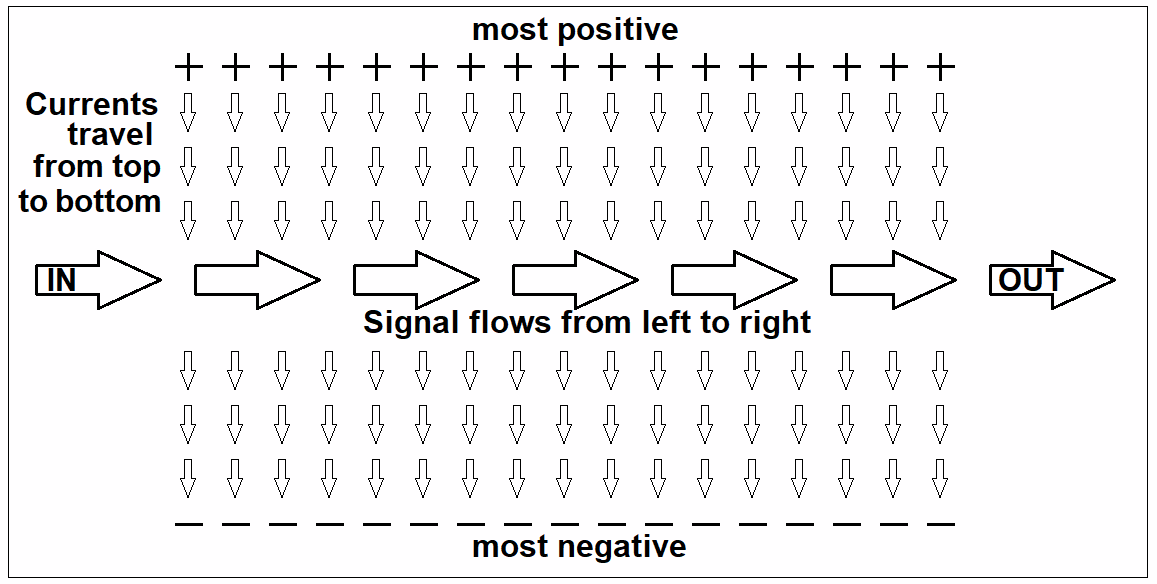
It also helps to re-orient schematics to follow a certain pattern. Let me show you what I learned very early in a electronics drafting class I took at Tektronix:
The teacher instructed us to imagine each drafting sheet of paper like the above. Most positive voltage sources at the top, most negative voltage sources (sinks) at the bottom, and to imagine that currents travel from the top of the sheet downward to the bottom of the sheet "like a hanging curtain", he said. He then said that signals should arrive as inputs at the left side of the sheet to travel across the curtains of current (which he said provided the impetus to allow the signals to travel) towards the right side of the sheet where they leave as outputs.
He also then said that we should not "bus around power" with wires. He said that it wasn't necessary to show all the wires needed to make connections because they added unnecessary noise against the idea of understanding a circuit.
I write a little more about that experience here.
Re-drawing schematics
So, one thing I learned to do is to simply sit down and redraw schematics so as to follow the drafting rules I'd learned in class. I went back over many of my old schematics, ones that I didn't understand all that well at the time, and redrew them.
One by one, I found that I finally could see. My eyes had been opened and things began to make sense.
Articles in many of the electronics magazines of the time (web sites, today) were focused on builders and clearly not focused on teaching electronics. So I could forgive them their difficult schematics. But so many textbooks, which most certainly were trying to teach electronics, I found similarly terrible schematics.
Once I learned how to see, because of some great teaching in a Tektronix drafting class, I made it a firm and fast rule to redraw pretty much every single schematic I wanted to read. No exceptions, ever. Just the act, itself, of redrawing a schematic helped me to understand it better.
I'm writing all of this to make a sincere point. Get into the practice of redrawing schematics. And use the above sheet style to guide your hands as you do it. And read some of the rules I list here, too. They may help you.
Redrawing your schematic
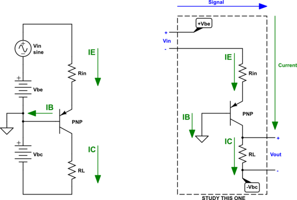
Something like this:

simulate this circuit – Schematic created using CircuitLab
On the left is your schematic, but now arranged per the sheet-and-signal-flow-model from Tektronix's drafting class. It's oriented better. But there are still too many wires.
On the right is the same schematic, but without all that wiring being shown. It's the same thing. No difference at all. But it is a little easier to start thinking about.
Note also that the schematic on the right has all currents pointing in the same direction, downward. And that the signal input is on the left side heading inward into the schematic and the signal output is leaving the schematic on the right side.
There's also simply less clutter.
You can easily see that the PNP emitter will be about one diode drop above the ground reference and that the power supply is bipolar (has a positive and negative voltage, plus a ground), with \$\mid V_{_\text{BE}}\mid \$ magnitude being the most positive and \$\mid V_{_\text{BC}}\mid\$ magnitude being the most negative. This means that the power supply has to provide a span of \$\mid V_{_\text{BE}}\mid+\mid V_{_\text{BC}}\mid\$.
That doesn't mean you will understand the circuit. That takes practice and learning about different topologies, one at a time, and acquiring these ideas in your head as you go.
Just redrawing isn't a magic wand. But it helps.
-
\$\begingroup\$ Actual, practical transistor circuits were often drawn with positive grounds in the 1950s. Using germanium, PNPs were easier to manufacture than NPNs, so they were less expensive and more common. NPNs were the upside down ones ツ \$\endgroup\$ Commented Sep 19, 2022 at 15:11
KVL and KCL do not require a reference node. You can remove the reference node entirely and still apply Kirchhoff's Laws. The reference is there so that single subscript notation can be used. For example:\$V_{C}\$ refers to the voltage from the collector node to the reference (ground) node.
-
\$\begingroup\$ It's generally more convenient to do nodal analysis (using KCL) after defining a reference node, because you have to in any case pick one node at which you will not write a KCL equation, to avoid producing a redundant equation. Mesh analysis (using KVL), as you say, does not require a reference node, or treat any particular node specially. \$\endgroup\$ Commented Sep 18, 2022 at 16:47
-
\$\begingroup\$ @ThePhoton: More convenient, yes, but not necessary. In general node labels are important for any analysis. The ground reference is a popular one for whatever reason. \$\endgroup\$ Commented Sep 18, 2022 at 16:55
-
\$\begingroup\$ The point is, if you use KCL you have to choose one node to treat different from the others. You don't have to choose the reference node or even define a reference node, but you do have to choose one node to be special. Using KVL, there's no special node. \$\endgroup\$ Commented Sep 18, 2022 at 16:58
-
The reference node being connected to the positive terminal seems wrong.
It isn't and you should teach yourself not to be bothered by it.
First, as other answers said, the results of circuit analysis using Kirchhoff's laws don't depend on the choice of the reference node.
Second, there's nothing special or unusual about having a node with a voltage below that of the reference voltage, and you should get used to analyzing circuits where that occurs.


