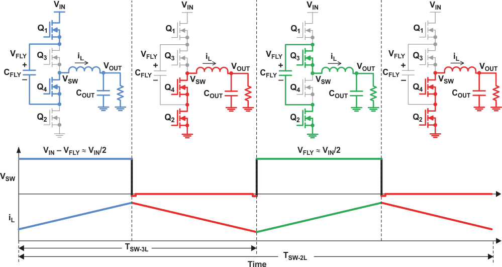
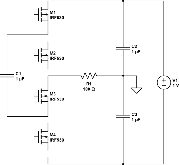
It might help if you looked at those diagrams as having the full Vcc applied between top and bottom, but the bottom is not grounded -- instead, Vcc has an additional capacitive divider with its middle point grounded:

simulate this circuit – Schematic created using CircuitLab
Now it should be more clear that the voltage applied per one leg of the half-bridge is Vcc/2. I've left M2 and M4 disconnected, it's intended, to show how the connections go for the first picture in the OP: M1 and M3 are closed so the voltage across them is zero, while C1 sees the full voltage of C2, before discharging on the load. The bottom switches (M3, M4) have the negated command pulses seen by the top. The other four steps should see the transistors switching each once, not all at once, not more than one at a time (think Johnson counter). I've only recently read about these things and, as I understand it, there can be more than one way to drive these but, the effect is that the switches have reduced voltage across (halvened in this case) and the effective switching frequency is N-1 levels times the carrier. E.g. for a 3-level, N-1=2 so the effective switching frequency is twice the carrier, resulting in lower losses and reduced values for the output filter. The downside is the number of switches (and capacitors). These applications make sense for high voltage, not high current (polyphase is a better choice then).
[edit]
First, note this key quote from TI's site (emphasis added):
By maintaining the flying capacitor balance at half the input voltage, the switch node can be presented with V IN, V IN over 2, or ground. Hence the name 3-level converter.
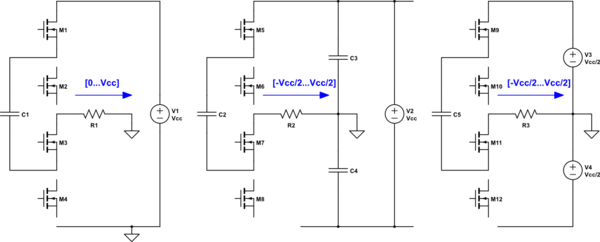
That's one clue. Then, in case the words in the comments were not enough, below is how the schematic in the OP transforms to the one above.

simulate this circuit
The 1st schematic to the left is the one in the OP and the load sees a voltage ranging from [0...Vcc], with a virtual modpoint at Vcc/2. If you transform this into the 2nd schematic you get the same voltage swing across the load but now, the midpoint is the actual ground, while the output can be negative. And the 3rd one is the same as the 2nd, except you're using two sources of Vcc/2, instead of only one of Vcc and two capacitors.
The reason for this transformation is to show why the flying capacitor charges at Vcc/2:
- in the 1st one it's not immediately obvious because the load seems to take the full
Vcc across it. But then it charges/discharges in a PWM fashion, so there will be an average.
- for the 2nd and 3rd it's clear that the capacitor can only charge at
Vcc/2, and then is discharged at -Vcc/2, same PWM involved.
It should be clear that the voltage across the flying capacitor can exceed, or go below Vcc/2 (also see the example in the comments) but, keeping it at Vcc/2 is optimal. This is for a buck converter, in the case of an SPWM, things change (the modulation index varies).
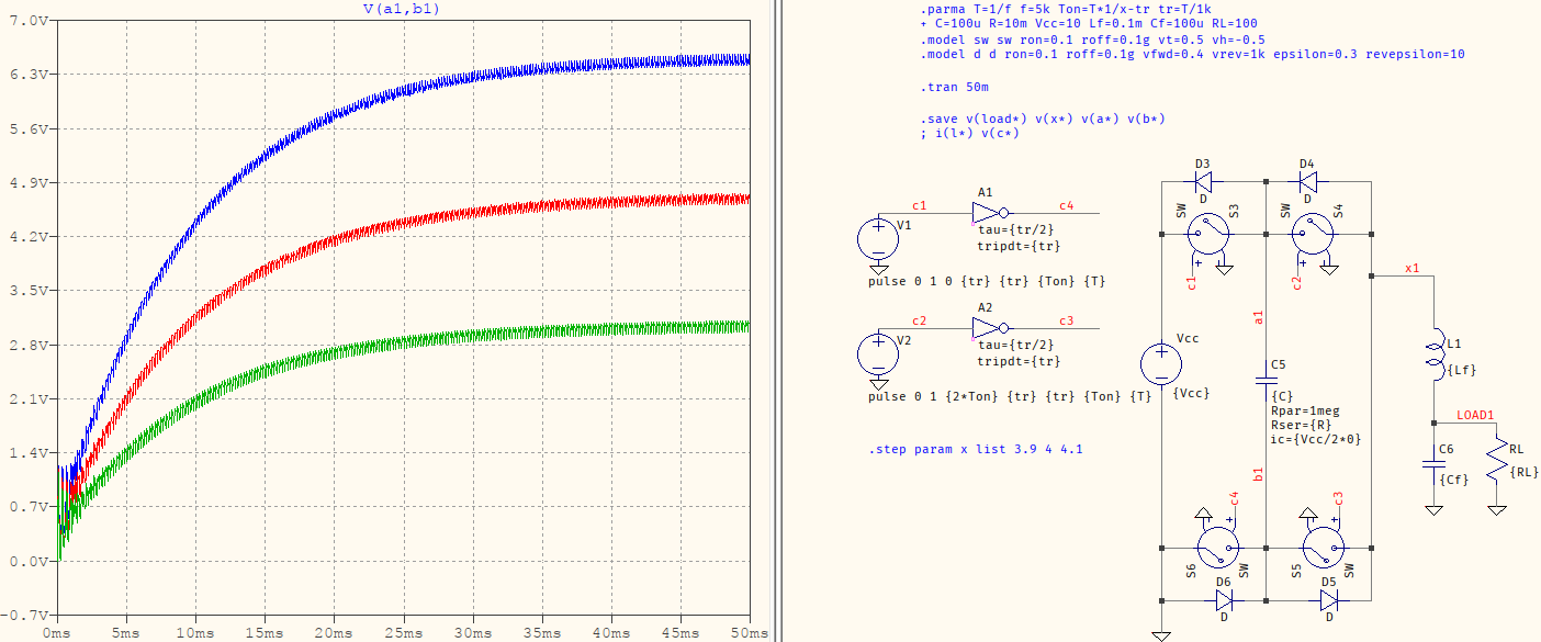
And, as always, you don't have to take my words for it, use a SPICE verification:

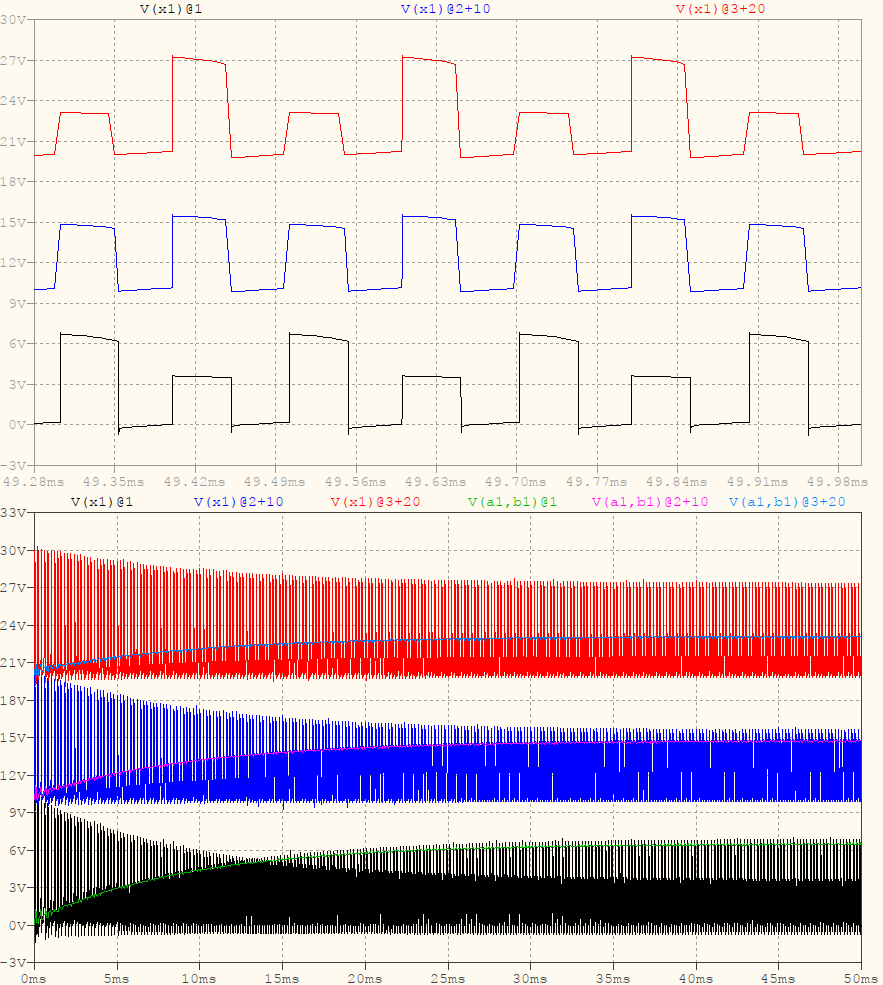
Ton is varied to be either ¼ of T, or slightly below/above. The result is that V(a1,b1) (the voltage across the flying capacitor) varies at Vcc/2, or above/below. With a balanced drive, the voltage is maintained at Vcc/2. When the output voltage varies, the duty cycle will need to vary but, even at that point, it will try to maintain a voltage of Vcc/2 or close to it. And the reason is to have the output pulse swings as even as possible:

At the top you see the voltage at the midpoint of the half-bridge. The blue trace is balanced: the pulses are closely matched in amplitude resulting in an even current through the inductor (which, as the TI video states, results in a peak current of 25% that of a regular buck converter). The black and red traces are the imbalanced ones and the effect will be higher peaks in the inductor current. At the bottom, the traces may be a bit harder to see but, they are shown as the voltage across the flying capacitor charges (see the light blue, pink, and green traces), overlayed on the waveforms of the half-bridge midpoints (all of them have some offsets for better viewing).
TLDR:
- The voltage across the flying capacitor is maintained at
Vcc/2 because that provides the optimal output/losses/efficiency/etc
- The reason I showed that topology in the 1st picture was for an easier viewing of how the supply voltage charges the capacitor (direct charge from the source/capacitor, compared to the averaged
Vcc).
And the reason I started with the 2nd point was because I assumed that, since the TI video (which you say you viewed) states, in clear, several times, that the voltage across the flying capacitor is maintained at Vcc/2, I didn't think that was even a problem. At any rate, now I've added that bit, too.

