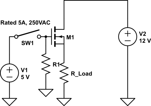
As the switch opens, the gate's capacitance will already have charged to +5V, the same as the +5V supply that charged it. That capacitance will tend to hold it there. Potential difference across the switch is therefore close to 0V immediately following the opening of the switch, and no arc will occur.
The same can't be said for closing, though. In your current implementation, the switch connects the 5V supply directly across the MOSFET's gate capacitance; the initial potential difference across the switch will be 5V, and initial gate charging current could be an ampere or more.
Potential difference isn't really a problem, as most switches will have a DC voltage rating between 2 and 10 times lower than their AC rating. In this application, DC voltage is 50 times lower. Current, though, might be a problem.
I would aim to keep current under 10% of the rated value, at 500mA or less. Considering you are using a pull-down resistor to switch off the MOSFET, which will necessarily slow down the switching process, I presume you are OK with similar performance while switching on, which permits us to use a resistance to limit gate current while charging.
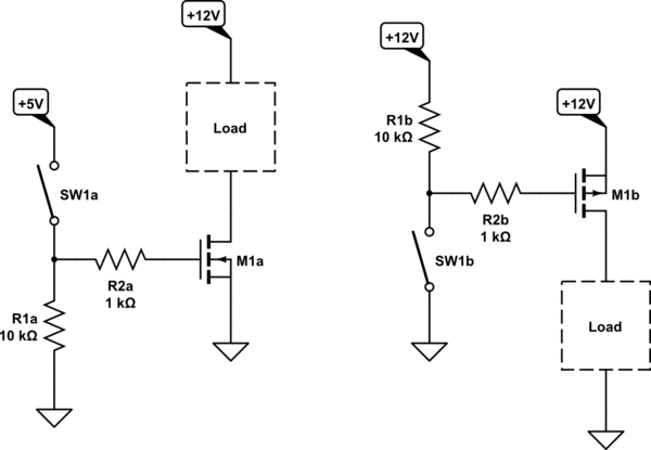
Gate capacitance represents a short-duration short circuit, when the switch is closed, which is bad for the 5V supply (and anything else connected to it), so limiting gate current is beneficial in that respect too. I suggest these designs, which deal with several issues:

simulate this circuit – Schematic created using CircuitLab
In both circuits I use R2 to limit gate current.
On the left, when the switch is closed, current through it peaks at \$\frac{5V}{1k\Omega}=5mA\$, but settles down to \$\frac{5V}{10k\Omega}=0.5mA\$ once the gate has charged, after a few microseconds. These currents won't cause the switch any harm, at least, not as much as switching an amp at 250V AC.
The circuit on the right will have switch currents over twice that (since I use the +12V source to charge the gate), but still well within our 10% bounds.
On the left I use an N-channel MOSFET, switching the low side, and on the right there's a P-channel device switching at the high side. Notice how both are connected common-source. In your own circuit, which is common-drain (source follower), the source is always \$V_{GS(TH)}\$ lower than the gate, giving rise to the "following" action.
That means, with the gate at +5V, the source is only \$+5V-V_{GS(TH)}=+3V\$ or so, not what you intended. To use a common-drain MOSFET as a switch in this application, you require a gate potential well over +12V, probably +16V or +20V, depending on the MOSFET model.
If you need the load connected to ground, switched high-side, then either use use an N-channel transistor as in your original configuration (common drain) with a gate potential switched between 0V and over (\$+12V+V_{GS(ON)}\$), or use a P-channel one, switched with +12V and 0V, as shown right.


