0
\$\begingroup\$

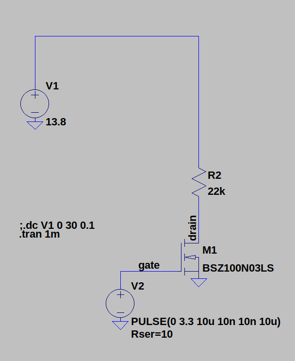
LTSpice circuit diagram

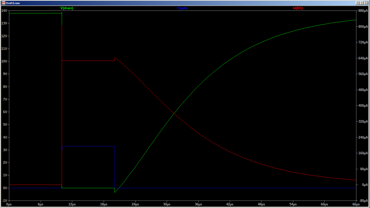
LTSpice simulation results

Hi folks, I'm simulating this very simple common source circuit with an NFET, with a pulse input on the gate input. On the falling edge of the gate voltage, I see a small negative output excursion on the drain terminal of the FET.

I'm wondering why this is occurring.

The green plot is the drain voltage, and you can clearly see the negative excursion right after the gate voltage goes down.

\$\endgroup\$
1
  • \$\begingroup\$ Might be the drain terminal inductance that's energized due to the constant drain current charging the drain capacitance? \$\endgroup\$
    – hatsunearu
    Commented Jul 6, 2023 at 5:19

1 Answer 1

3
\$\begingroup\$

There is drain-gate capacitance (also called reverse transfer capacitance) and your transition is fairly fast (3.3V in 10ns).

Doesn't matter with 22kΩ load, but note that 3.3V is not really enough gate drive for that part if you want very low Rds(on).

If you reduce the drain resistor to (say) 100Ω the negative-going bit should largely or entirely disappear.

\$\endgroup\$
1

Your Answer

By clicking “Post Your Answer”, you agree to our terms of service and acknowledge you have read our privacy policy.

Not the answer you're looking for? Browse other questions tagged or ask your own question.