2
\$\begingroup\$

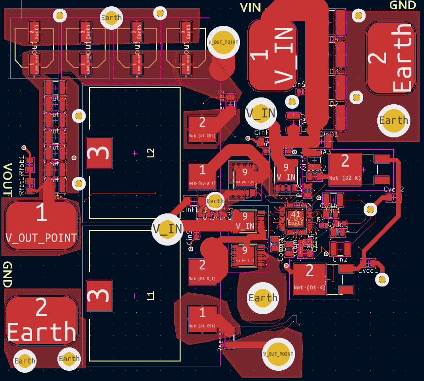
Thanks to your advice on StackExchange, I'm in the final stage of developing my first LM5143A-Q1-based (link to datasheet) buck converter! It may be a bit rushed as I need to prepare this for a high school project and I'm still learning, but positive criticism is highly welcomed! The problem now is, routing. I would appreciate it a lot if you could take a look at it and tell me if there are any issues. What could be improved?

EDIT: High Quality (.SVG) images are available to download at this link. I wanted to place them in this post but the website doesn't accept this format.

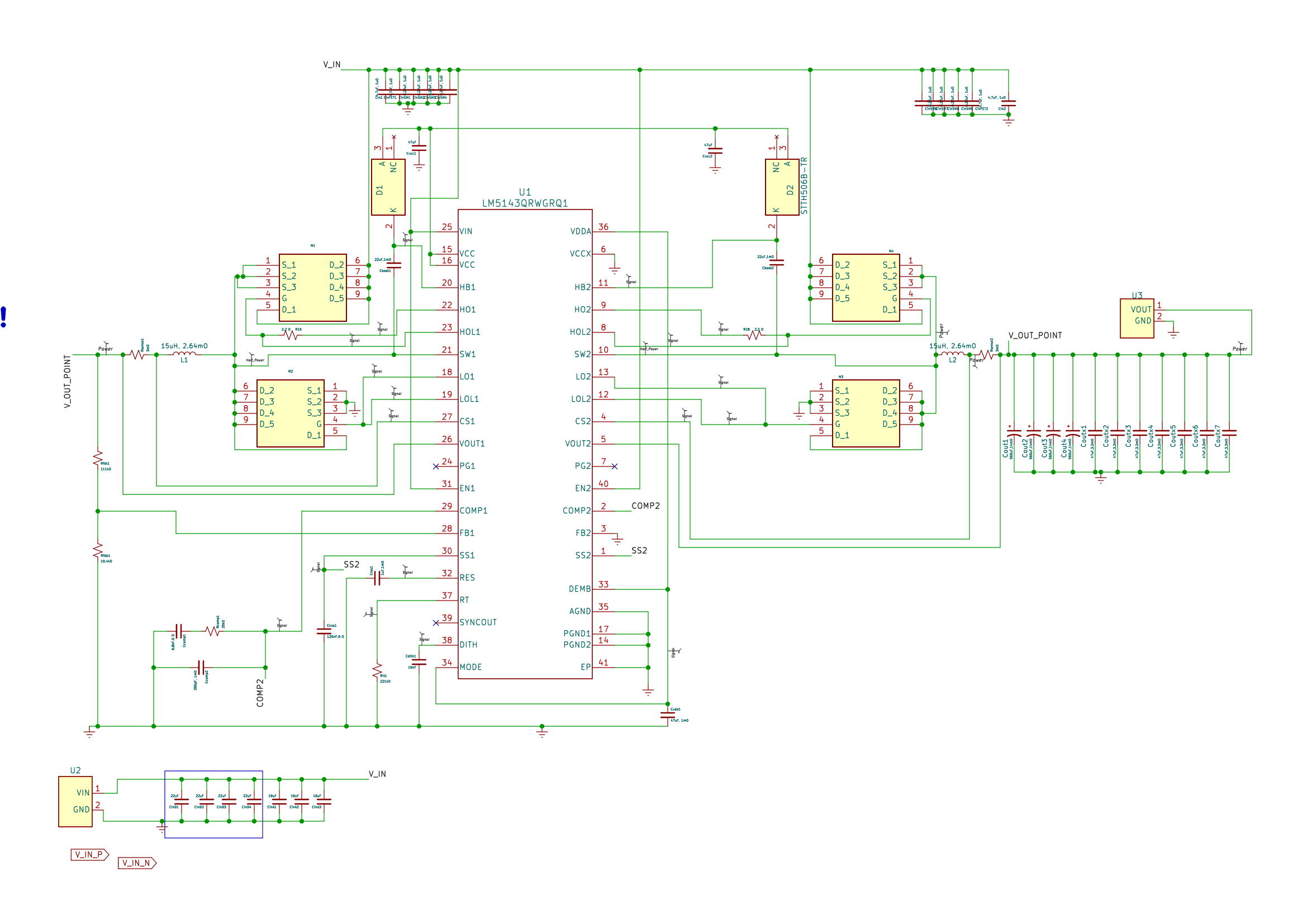
This is the schematic, all done in Kicad: Schematic of buck converter
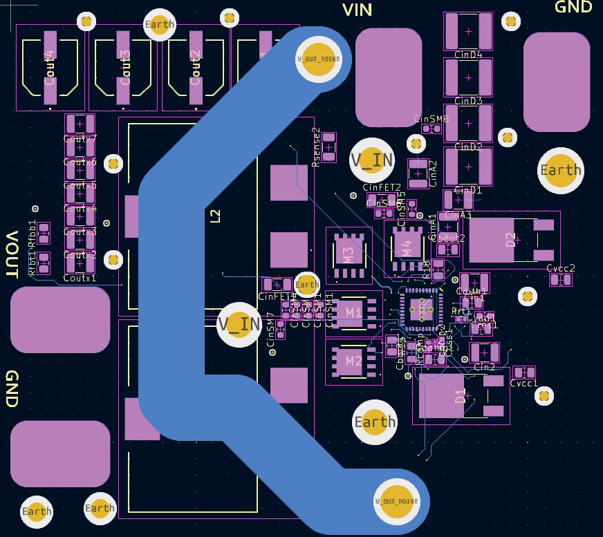
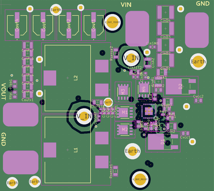
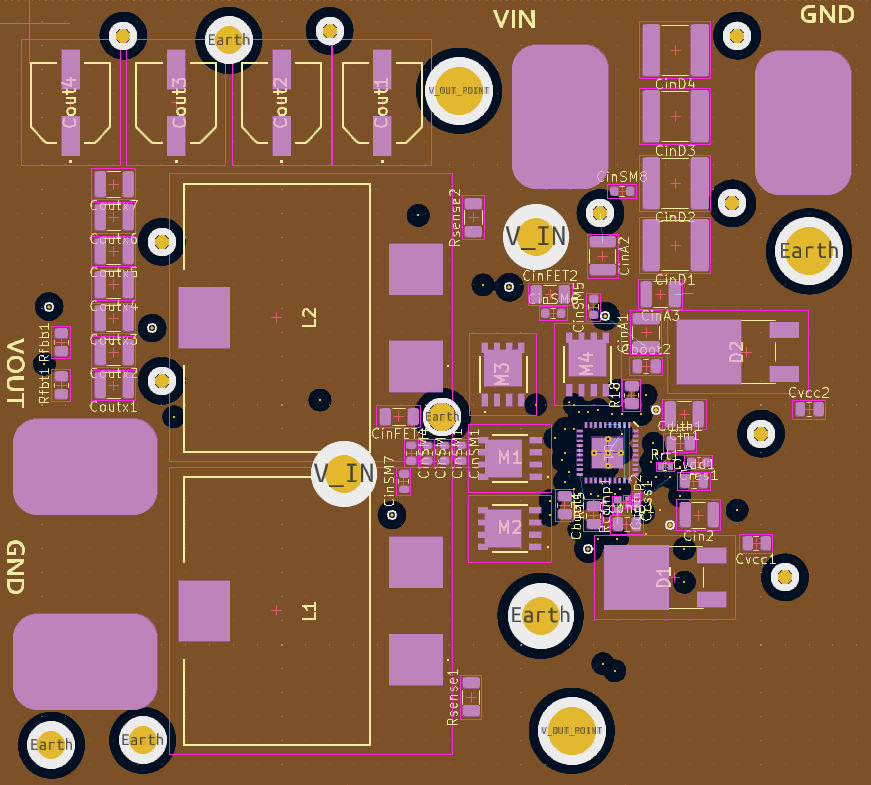
This is the layout: Top Layer, all components mounted here

All components mounted

GND Layer GND layer, tried isolating the big VIN vias more

VIN Layer The VIN layer

The Bottom Layer, yes, big trace Bottom Layer

There are a couple of quick questions I have about the visuals:

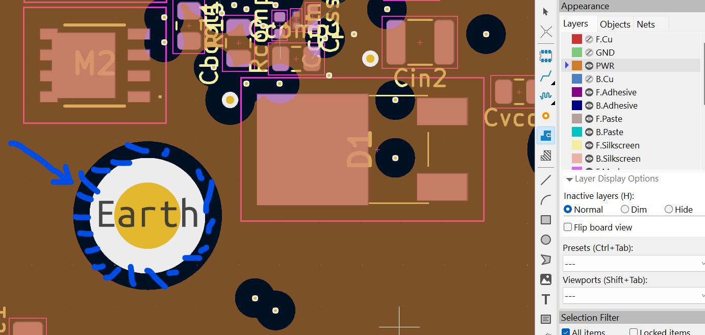
  1. Take this via for example. Does the black area between it and the PWR (VIN) plane mean it's isolated from the plane? Else it would be shorted! enter image description here
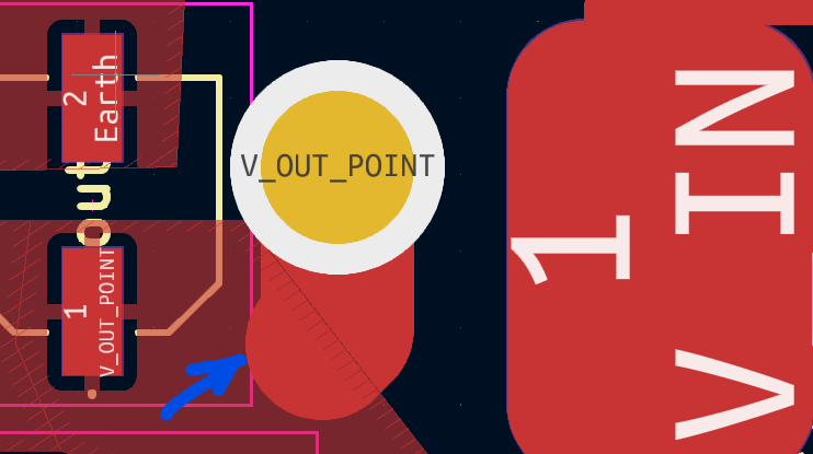
2.Take this via for example. If the standard trace goes into the filled zone, does that mean it's making contact and they're connected? Since it should Trace into filled area
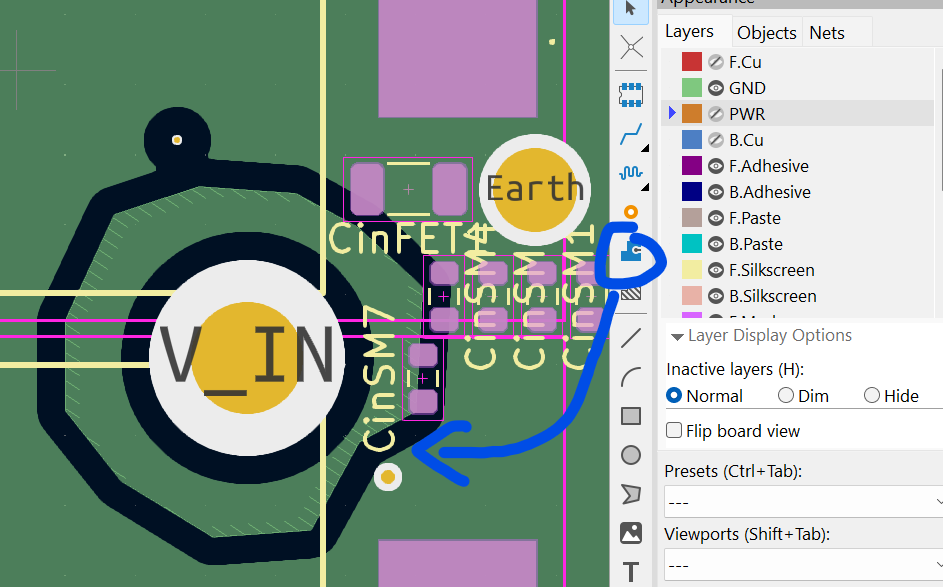
  1. If the via is itself isolated, is there any reason to make another isolation copper island like in the photo below? Copper Isolation
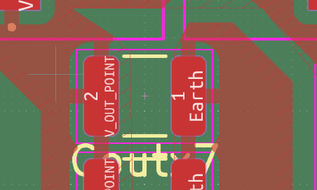
  2. Is there any reason to use these "thermal reliefs" over standard tracks? (I did it since I heard they're good) Capacitor example
The layout was highly inspired by Brian's 4 layer board. (except from his perfect copper islands) From him and all the resources I searched, I understood a couple of basic design rules:

  1. Ground Plane always underneath IC
  2. Keep traces as short as possible (well, except for that huge L1-L2 connection on the back... How big of a problem will it be?)
  3. Use filled zones instead of traces when possible
  4. Keep all high freq parts on the same side

Thank you in advance for any advice! It's the first time I'm doing something like this and I loved learning it!

\$\endgroup\$
7
  • \$\begingroup\$ If you can import an higher resolution picture of the board, it will be easier to review \$\endgroup\$
    – Julien
    Commented Jul 26, 2023 at 22:02
  • 2
    \$\begingroup\$ When I see a lack of a ground pour on the top layer, I find the layout suspect for a switching power supply. Look at the layout suggestions in the data sheet starting on page 53. PCB layout diagrams start on page 56. There is also an evaluation board for this product with PCB layout files. This is a proven design. Avoid using thermal reliefs on switching supplies. If your soldering iron can't handle it, preheat the board. \$\endgroup\$
    – qrk
    Commented Jul 26, 2023 at 23:07
  • \$\begingroup\$ A couple of general observations as I have not researched this part yet: What powers VDDA, DEMB, and MODE? Are COMP1 and 2 supposed to be tied together? And what happens when FB2 is grounded? If at all unsure, consult the device datasheet. Double and triple-check everything. \$\endgroup\$
    – rdtsc
    Commented Jul 27, 2023 at 0:43
  • \$\begingroup\$ @Julien I just added a link to higher resolution .SVG images for each layer \$\endgroup\$
    – Mito
    Commented Jul 27, 2023 at 13:36
  • \$\begingroup\$ @qrk Is it mandatory to have a ground pour on the top layer if there's a ground layer right underneath the top? And why should thermal reliefs be avoided though? I could indeed just place the PCB on a mini hotplate and then solder (what can be soldered) by hand \$\endgroup\$
    – Mito
    Commented Jul 27, 2023 at 13:53

2 Answers 2

3
\$\begingroup\$

A couple observations: the DRC will answer a lot of these questions. If you have a trace going to a polygon on the same net but for some reason they're not connected, DRC will tell you. If you have a via or hole touching a trace or poly it's not supposed to, DRC will tell you, assuming you have your rules set up correctly. Your silkscreen is going to pop a lot of errors; it's easier to lay out your components the first time with silkscreen in mind rather than do a major redesign just to make designators visible.

You do not need the extra isolation around the vias. The black ring shows you that nothing will touch it (make sure all your copper layers are visible). A lot of them seem oddly sized, make sure your board fab house can handle them. If you plan on using them as plated through-holes for wires, then make them actual 1x1 PTH instead of giant vias. I can see several that will be unusable once components are populated. If they are supposed to be vias, the usual way is to add several instead of one giant one.

A lot of the polygons are oddly shaped and only half-intersect with the things they're supposed to. Sometimes you can't make everything look pretty but e.g. that poly for Earth on the lower left could use some love.

What is Earth? I don't see it anywhere on your schematic. If you mean GND, then make it one net only.

How are you planning on soldering this? If you are using a hot plate, then thermal reliefs are not necessary, but make rework easier. If you are using an iron and/or hot air then they are. Critically, your high current input/output pads are connected to huge polys and traces with four spindly thermal relief spokes.

Speaking of spindly, the traces on the bottom layer seem narrow. Like unmanufacturable narrow.

I would suggest looking at the datasheet for the chip, specifically the "layout" section. Power switchers are a bit picky about their layout. You're learning, which is great and this isn't a knock on you, but I doubt this board will function as it is currently laid out.

Finally, it doesn't look like you've taken thermal considerations into account. Page 56 of the datasheet describes how to remove heat from the exposed pad on the underside of the package using vias to a ground plane, which is missing from your design. There are other components that would probably benefit from being attached to a plane as well.

\$\endgroup\$
3
  • \$\begingroup\$ Well that sure is a lot of DRC errors (264 , 291+Warnings)! I'll have to look at this. And yes, vias are supposes to be normal vias, not a PTH (What is that?). I didn't know the best way is to have multiple small vias instead of just a big one. I'll try to see if I can split them. I tried my best to make them look as pretty as possible, but I'm a bit hesitant to extend them too much just for beauty. Also Earth is GND. I just used the earth symbol in the entire schematic. I'm planning to use an mhp30 mini hot plate with solder paste and a stencil, anything else will be done with an iron. \$\endgroup\$
    – Mito
    Commented Jul 27, 2023 at 14:15
  • \$\begingroup\$ What do you mean by "spindly"? All small traces are of 0.15mm. I'm planning on ordering it from JLC PCB and their (minimum trace width)[jlcpcb.com/… is 3.5mil/0.09mm, so it's fairly away from the minimum. The small vias are a bit more critical, as they're 0.2/0.4mm and the minimum is 0.2. And I did look at the datasheet "layout" section, but I didn't fully understand it then, now I get it! They use huge copper islands insulated from each other for GND (low side) and VIN (high side)! Did I get it right? \$\endgroup\$
    – Mito
    Commented Jul 27, 2023 at 14:27
  • \$\begingroup\$ Also not only that but it seems they connected the drain and source between the mosfets using an island as well! Another question: Why did they use the "dotted rectangle area line" "GND pad geometry" there? They "Isolate" the switching area and reduce EMI? As for the thermal considerations, I'm not sure if it's that simple. Like, do vias connected to the underneath GND layer and nothing else really help with heat management? I see for example the back of the IC has 5 vias with no net, but the back is supposed to go to GND, so should I assign them the GND (Earth) net? \$\endgroup\$
    – Mito
    Commented Jul 27, 2023 at 14:38
1
\$\begingroup\$

First of all, good job!

I'm not an expert in KiCad, but whenever you have such question, you can check the gerbers. They never lie since it's the file your manufacturer will use!

Here are the answer to your questions:

1 Take this via for example. Does the black area between it and the PWR (VIN) plane mean it's isolated from the plane? Else it would be shorted! -> Yes it's isolated from ground.

2.Take this via for example. If the standard trace goes into the filled zone, does that mean it's making contact and they're connected? -> I would say so, but be careful, based on other software (Altium) the behavior when repouring might surround your trace. Here it doesn't seem to be an issue.

  1. If the via is itself isolated, is there any reason to make another isolation copper island like in the photo below? -> Not to my knowledge. I'm not working in very high voltage, but I don't see any reason to place that (except plane filling FYI-> when you have 8+ layer, you must ensure all your plane have copper on so the PCB remain flat)

  2. Is there any reason to use these "thermal reliefs" over standard tracks? (I did it since I heard they're good) -> Thermal relief are very important whenever a huge part of copper is connected to a pad. Either a plane or a trace. Otherwise, it will be very hard to solder since the pad will remain cold. Not having thermal relief can also make component stand up.

Here are some of my comments on your layout

All the rules you have listed are good in general design. So, why did on the bottom layer didn't you place a plane!? (It's large, yes but it can be larger!)

Having huge vias, in general is not as good as several smaller. The impedance of one large via can't match 20 smaller one.

Your power plane (Vin) is highly degraded near the IC. I don't know your clearance constraint but they seem a bit loose which make the plane weaker.

Usually, you would want your stackup for a four layer to be (top to bottom) Components and most traces, GND, PWR, Rest of traces. The reason why this is the best topology is that the most trace are close to the gnd which give them a better impedance control. Also, it increase the capacitance between the GND and supply (this is the best decoupling capacitance since it has a very low ESR). Finally, it allow a way easier debugging since you can cut trace (I once had to cut a trace on a third layer, you don't want that!).

You have some very narrow trace that are quite long. I'd make them a bit wider so they are less lossy.

You seems to have some very small vias. Even if not a lot of power goes tough them, they are harder to manufacture and will increase to a more expensive board and a higher failure rate.

I haven't review the layout. With a quick check, I think your output capacitors are way to far away from your chip, but I'm unsure.

If I had an advice to give you is to get the best PCB design, spend as much time doing and redoing your component placement. That's what makes the difference! And with practice, it will take you less and less placement to have a good and neat PCB.

The image is too pixelized for more comments, but I'm impressed! I have seen worst from actual PCB designers!

\$\endgroup\$
9
  • \$\begingroup\$ Regarding the 4L stackup, SIG, GND, PWR, SIG isn't great; you're better off using SIG+PWR, GND, GND, SIG+PWR to ensure solid reference planes for everything. Routed power instead of power planes on inner layers should be fine unless you need tens of amps. The Extreme Importance of PCB Stackup by Rick Hartley is an excellent talk on this subject. \$\endgroup\$
    – Polynomial
    Commented Jul 26, 2023 at 22:23
  • \$\begingroup\$ If your PWR plane is weak, it's has bad has if your GND plane is weak. I don't have an hour right now to check if Rick Hartley justification, but a power plane can't be cut by traces. It would increase it's inductance quite significantly. Can you explicate why he suggest that power on top and bottom with traces is better? \$\endgroup\$
    – Julien
    Commented Jul 26, 2023 at 22:33
  • \$\begingroup\$ The extremely short version is that electric energy travels in the fields in the dielectric space between a conductor and its return path, so you want a reference plane (typically ground) physically close to every current-carrying conductor. On a 4L stackup the spacing across the core is much larger than the outer layer spacing, so that's a factor, and if you do SIG/GND/PWR/SIG you end up running your bottom layer signals' return currents across the power plane and spreading the fields out as they search for a low impedance return path, which is bad for both conducted and radiated emissions. \$\endgroup\$
    – Polynomial
    Commented Jul 27, 2023 at 0:55
  • \$\begingroup\$ I would highly recommend watching the linked talk, though. Probably the best electronics talk I've ever watched. \$\endgroup\$
    – Polynomial
    Commented Jul 27, 2023 at 0:56
  • \$\begingroup\$ I think we are getting off topic. If you want to continue the discussion, I think we should open a new question. \$\endgroup\$
    – Julien
    Commented Jul 27, 2023 at 12:28

Your Answer

By clicking “Post Your Answer”, you agree to our terms of service and acknowledge you have read our privacy policy.

Not the answer you're looking for? Browse other questions tagged or ask your own question.