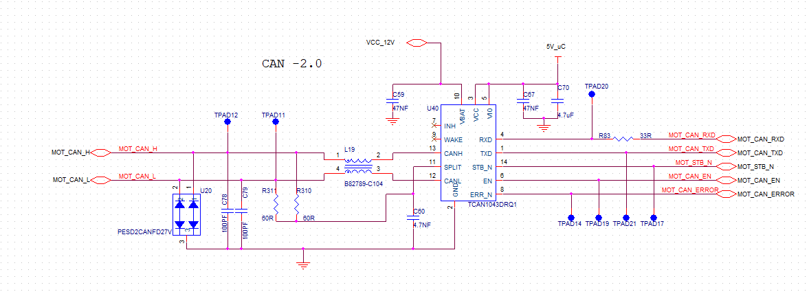
CAN bus is very low edge rate. It's highly unlikely that you'll ever have a PCB large enough, to have traces long enough, with such a stackup that the trace impedance will be woefully out of spec. Just choose a trace width in the right ballpark, no need to order with controlled trace impedance.
Average digital logic traces are in the 50-100 ohms range, typically near or at the minimum design rules for the fab (4/4 mils on thin (4-7 mils) prepreg, 7/7 mils on medium (7-10) prepreg). This suffices for the logic signals.
Put two such traces side by side, and that's 100-200 ohms differential (they hardly couple together). If you're on the low side of that range, congratulations, you have a CAN pair!
If the electrical length of that pair is a fraction of a bit time, and the total bus and stub length is still adequate for the given baud rate -- CAN won't care. It's very robust to poor media.
In the interest of good signal quality, we should of course save error budget where possible, in case other devices perform worse, and to maintain a greater margin when things do break down. Simply choosing the low end of that range will be fine, and we don't need impedance control for that. Further, choosing relatively short trace lengths, even when the impedance is woefully mismatched, keeps the total effect low.
Just to put trace length in context: at minimum design rules 7/7 (mils), on a sheet-of-paper-sized PCB, you could draw about 300 zig-zags back and forth, of 11" each, or 84 meters (or slightly different numbers for a proper sheet of A4). At 65% c, that's 0.43µs, or 43% of a bit-time at 1Mbps. So, even long buses making long routes around a board (just not doubling back on themselves dozens of times like this!) will hardly have an effect on the fastest CAN (5Mbps?), at least in terms of edge quality.
Keep in mind, trace length adds to overall bus/stub length, which is limited by baud rate. Common mode chokes also have some electrical length which should be added (but, is rarely if ever specified about the component; it can be estimated from the leakage inductance where available).
As for power supply traces, these don't matter as long as the bypass caps are placed locally, and they can be connected to the device with somewhat wider traces (10-20 mils). If using inner plane power, place the via(s) nearby -- where, which side of the pad(s), doesn't really matter. If routing on a signal layer, use adequate width for the current rating. Which should be pretty low (100s mA at most?) so it doesn't matter much.
Do mind that trace length corresponds to inductance (low frequency equivalent), which can cause bypass capacitors to ring against low-impedance nodes elsewhere in the power distribution network (PDN). This can be estimated by inspecting the layout, and converted into a simulation to show the frequency response. A possible outcome of this is adding bulk capacitors (relatively large values (several times the total local bypass) with selected ESR) in strategic locations, to dampen the PDN.

