1
\$\begingroup\$

I am studying the schematics of an analog isolator with variable gain SIM 984 from SRS, the isolator is bipolar and can handle positive and negative voltages.

In the isolation part of the schematics (see picture below), the author uses two voltage references circled in red.

Having read the manual of the analog optocoupler used here (HCNR200) I think that these are used as current sources and make the whole device effectively bipolar. Their role I think is to make sure that the current flowing through the photodetectors on the input part is always positive. See p.19 of the HCNR manual (https://docs.broadcom.com/doc/HCNR200-HCNR201-High-Linearity-Analog-Optocouplers-DS) where it reads:

The circuit in Figure 15a uses two current sources to offset the signal so that it appears to be unipolar to the optocoupler. Current source IOS1 provides enough offset to ensure that IPD1 is always positive. The second current source, IOS2, provides an offset of opposite polarity to obtain a net circuit offset of zero. Current sources IOS1 and IOS2 can be implemented simply as resistors connected to suitable voltage sources.

The thing is, on the input side for example, the voltage V_in can reach up to +/-1000V according to my understanding of the device, and given the input resistor the current can reach +/-10mA. So if say the current reaches -10 mA the voltage reference must source 10 mA for the current to stay positive, this is because I am assuming the op amp to be ideal and that no current flows into the inputs. But at best the current sourced by the voltage reference is 5/38300<<10 mA. So how does this work ? Am I completely mistaken in the role of the voltage references ?

The full schematics can be found on (https://xdevs.com/doc/Stanford_Research_Systems/SIM900/sim984_sch.pdf)

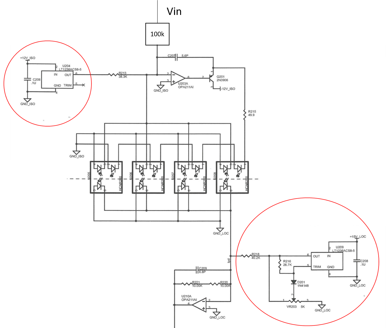
enter image description here

\$\endgroup\$

1 Answer 1

3
\$\begingroup\$

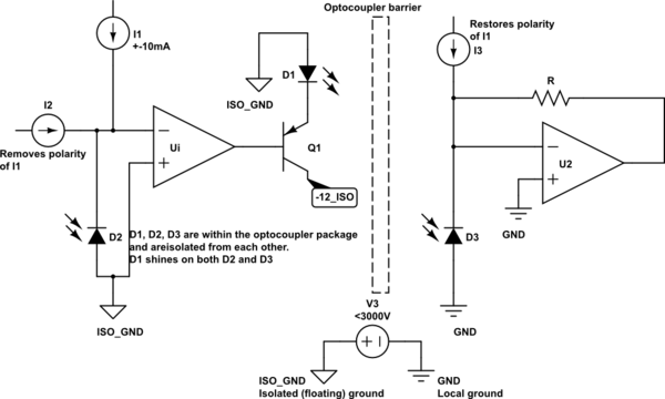
A simplified circuit diagram is shown below.

The designer used four optocouplers to obtain a current range more suitable for the feedback diode.

The optocoupler photodiodes used for feedback are all in parallel and so are represented by a single photodiode D2 with 4 times the current capability.

The photodiodes on the other side of the barrier are also in parallel so are represented by a single photodiode D3 with 4 times the current capability.

The emitting diodes are connected in series so to keep the current through each emitter identical and so the transistor need not supply 4 times the current. The are represented by D1.

The circuitry in the small red circle is represented by the current source I2, The input voltage and the 100k resistor are represented by I1. and finally the circuitry in the large red circle is represented by I3.

But at best the current sourced by the voltage reference is 5/38300<<10 mA. So how does this work ?

The missing current is supplied by the feedback diode. I2 is chosen so that when the input current is -10mA, the current through D2 is zero. (Maybe a little higher). The photocurrent is directed from cathode to anode, so pulls current from the input node,

If I1 = -I2, then opamp feedback action will force the photodiode, I_D2, current to zero. Since the diode D2 current comes from the light falling on D2, then the light falling on D3 will be the same by design of the optocoupler.

When I1 is properly selected, the current through the emitter will always be positive. The midpoint current represents 0 volts on the HV input.

So then the light falling on D2 and D3 represent the -1000 to +1000 volts of the input. Thus the current generate by D3 also represents the same voltage range.

The transimpedance amplifier converts I_D3 to a voltage. The bias current I3 is chosen so that the output voltage is 0V for HV=0.

The feedback resistor is chosen for the desired output voltage based on the input range.


Am I completely mistaken in the role of the voltage references ?

No. Together with the op-amp input resistors. They provide the desired offset.

I did not do any calculations. But the component values don’t seem to work for a -1000V input.

Checking the full schematic diagram, the Vin is likely to be no more than about 10V. This would bring the current into range.

schematic

simulate this circuit – Schematic created using CircuitLab

\$\endgroup\$
8
  • \$\begingroup\$ Thank you very much for this excellent answer @RusselH. I have a few questions regarding your answer, when you say If I1 = I2, then opamp feedback action will force the diode current to zero. do you mean if I1=-I2 ? and by diode do you mean the one emitting light (the LED) ? \$\endgroup\$ Commented Aug 8, 2023 at 15:24
  • \$\begingroup\$ Also, I was wondering about the use of the transistor, you are right in saying that it does not need to source 4 times the current, in this case I wonder why it is used, I had assumed it was because the OP amp could not supply enough current but when I looked at the data sheet of the op amp (OPA 211), it says that its typical output current is 30 mA which should be more than enough for the LEDs in series given the range of currents we're talking about. Is there any other reason one would use a transistor here ? \$\endgroup\$ Commented Aug 8, 2023 at 15:24
  • 1
    \$\begingroup\$ Op-amp feedback action will force the photodiode D2 current to zero. \$\endgroup\$
    – user319836
    Commented Aug 8, 2023 at 15:55
  • 1
    \$\begingroup\$ "do you mean if I1=-I2 ?" Yes, I corrected. @UnstableDynamics \$\endgroup\$
    – user319836
    Commented Aug 8, 2023 at 19:57
  • 1
    \$\begingroup\$ "wondering about the use of the transistor". I suspect it is to reduce the Rout of the op-amp. Even though the op-amp can source 30 mA, the open loop Rout may be significant @UnstableDynamics. \$\endgroup\$
    – user319836
    Commented Aug 8, 2023 at 20:01

Your Answer

By clicking “Post Your Answer”, you agree to our terms of service and acknowledge you have read our privacy policy.

Not the answer you're looking for? Browse other questions tagged or ask your own question.