0
\$\begingroup\$

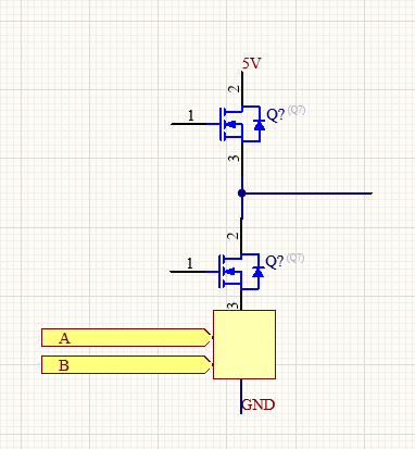
I want to add a circuit to my design in order to build a AND logic gate (preferably with MOSFETs) where in the next schematic you can find a rectangule. A and B would be the inputs, and the output would connect my circuit (the other two MOSFETs) with GND. I don't know how to accomplish this. I have found all AND gates are made using BJTs. enter image description here

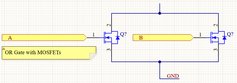
All I can think about a OR gate like this: enter image description here But I need a AND one.

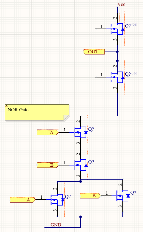
Another solution I found is a NOR gate (using active low signals in this case). I don't know if MOSFETS would work: enter image description here

\$\endgroup\$
1
  • 1
    \$\begingroup\$ "Basic" transistor gates invert: if you want both input&output "active high" (resp. low), you need more than one "stage". \$\endgroup\$
    – greybeard
    Commented Aug 23, 2023 at 13:52

2 Answers 2

0
\$\begingroup\$

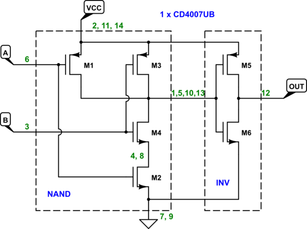
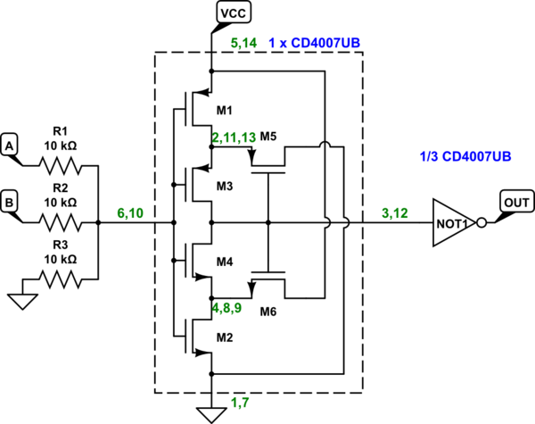
A 2-input and gate can be built with just 3 CMOS complementary pairs. You can get all of the transistors needed in a single package: CD4007U.
schematic

simulate this circuit – Schematic created using CircuitLab

M1-M4 make a 2-input NAND gate, followed by an inverter made of M5-M6. The green numbers indicate the pins of the CD4007U chip. When multiple numbers are listed, the pins should be connected together. E.g. pins 4 and 8 must be connected together (and to nothing else).

  • When either A or B are low, M1 or M3 are pulling the inverter input high.
  • When both A and B are high, M2 and M4 are pulling the inverter input low.

This behavior is that of a NAND gate. The inverter buffers and inverts the NAND's output, giving the same output as that of an AND gate.

I have found all AND gates are made using BJTs.

And those "gates" often work terribly poorly too, unfortunately. If you'd want performance similar to CMOS in terms of speed, then look for the schematic of the TTL 7408 AND gate.

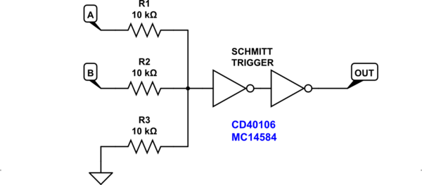
You can also implement an AND gate using a single Schmitt-trigger buffer - a CMOS equivalent of RTL (resistor-transistor logic):
schematic

simulate this circuit

A non-inverting Schmitt trigger requires 4 CMOS pairs. 3 pairs are used for the Schmitt inverter, and one is used for the output buffer inverter. So it doesn't make sense to design an AND gate this way since it performs just as relatively poorly as RTL did. We could call this architecture "RCL" - Resistor CMOS Logic :)
schematic

simulate this circuit

\$\endgroup\$
0
\$\begingroup\$

You can put your 2 NMOS in series. In this case the MOS will only create a low impedance path to GND when both A AND B are ON. Imagine B going high, bringing the source of the A-MOS to GND. If A then turns ON, it's drain will also be brought to GND. Of course the gate drive signals need to be referenced to GND as well.

\$\endgroup\$
3
  • \$\begingroup\$ Can I have problems having 4 MOSFETS in series? Due to references or anything like that. \$\endgroup\$ Commented Aug 23, 2023 at 12:58
  • \$\begingroup\$ Only the top most MOSFET requires a particular gate signal since it will be referenced to the output, i.e. if you want 5V out, you'll need to drive it's gate at >5V+Vgs_th wrt GND. The 3 "low side" NMOS will all turn ON with a standard GND referenced logic signal. \$\endgroup\$ Commented Aug 23, 2023 at 14:55
  • \$\begingroup\$ I would drive a PWM in the upper side. \$\endgroup\$ Commented Aug 24, 2023 at 6:27

Your Answer

By clicking “Post Your Answer”, you agree to our terms of service and acknowledge you have read our privacy policy.

Not the answer you're looking for? Browse other questions tagged or ask your own question.