2
\$\begingroup\$

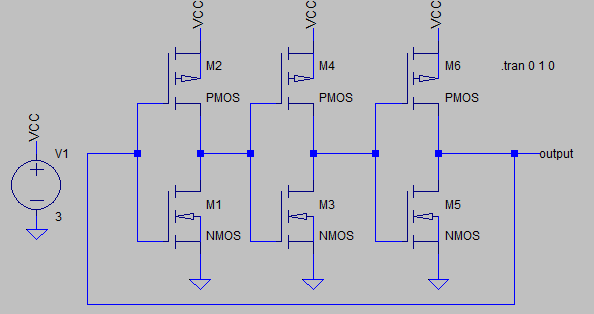
I am designing a ring oscillator using MOSFETS to create the inverters however, I am encountering problems with the output. Please check my understanding. Here is what I understand: the oscillating frequency should be:

$$F_{osc} = \frac{1}{2NT_{p}}$$

This is the most general case. To change the propagation delay, you can add load capacitors between each inverter stage and the frequency of oscillation can be calculated if you know the current through the transistor and the load capacitor. The frequency of oscillation becomes:

$$SlewRate = \frac{I_{ss}}{C_{L}}$$

$$T_{propagation} = \frac{V_{sw}}{SlewRate}$$

where $$V_{sw}$$ is the switching voltage of the inverter. And the equation for the oscillation frequency becomes:

$$F_{osc}=\frac{I_{ss}}{2NV_{sw}C_{L}}$$

And the inverter propagation delay is the average of the low to high and high to low propagation delay:

$$T_{prop} = \frac{T_{PLtoH}+T_{PHtoL}}2$$

So with all of this information, what I understood was that you can change the oscillation frequency by changing the supply voltage, the load capacitor, or by changing the size of the transistors. The supply voltage will change Iss. The load capacitor will change the slew rate which will change the propagation delay. Changing the size of the transistors will change the Iss current which will also change the slew rate which will change the propagation delay. Let me know if I messed up anywhere.

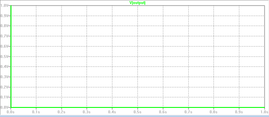
The next part is that if I want the output to swing from VCC/2 to VCC (I chose this arbitrarily not for any specific reason but to observe behavior), then I need to set W and L the same for both transistors. I did this and simulated the oscillator. The output is a flat line that doesn't oscillate. Here is the simulated output: enter image description here
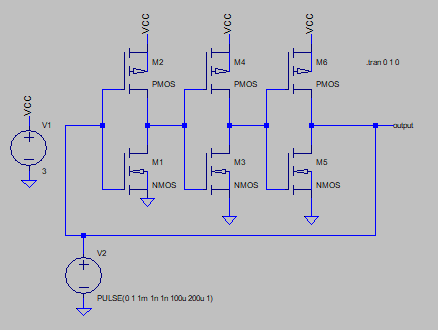
Here is the schematic:

enter image description here

I set w=50nm and L =1u. Can someone please explain why my inverter isn't oscillating and check if I made any errors with my understanding? I appreciate the effort. If any additional information is needed, please let me know and I will provide this information. The MOSFET models I am using are nmos4 and pmos4.

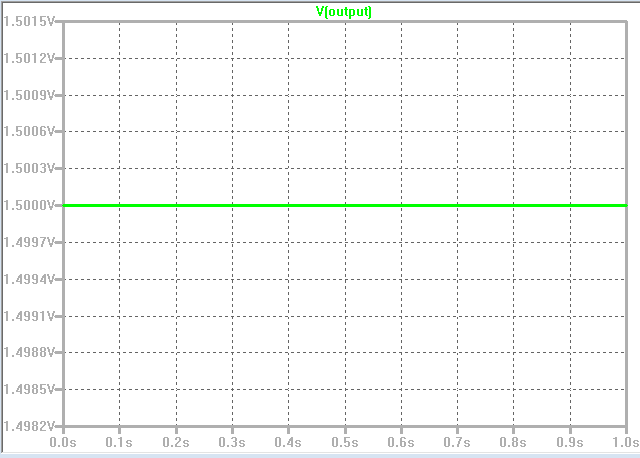
update: I added a pulse source on the feedback network and got this result

enter image description here

here is the schematic.

enter image description here

The circuit did not oscillate after adding a disturbance siganl. The disturbance signal was a pulse.

\$\endgroup\$
10
  • \$\begingroup\$ Why are you using the default MOSFET models? \$\endgroup\$
    – Hearth
    Commented Dec 1, 2023 at 21:01
  • \$\begingroup\$ I ran into a ton of issues with importing a model so I tried using the default models SPICE comes with. \$\endgroup\$ Commented Dec 1, 2023 at 21:14
  • 1
    \$\begingroup\$ Did you try adding a small step voltage in the loop? \$\endgroup\$ Commented Dec 1, 2023 at 21:47
  • \$\begingroup\$ A step voltage? I'm not sure I understand. I thought ring oscillators fed the output back to the input? without intervention of another source? \$\endgroup\$ Commented Dec 1, 2023 at 22:58
  • \$\begingroup\$ @spiderman19 The default model is usually not good for most uses, as it represents a very tiny FET inside an IC. You don't need to import a model; LTspice comes with a selection of common MOSFET models. \$\endgroup\$
    – Hearth
    Commented Dec 1, 2023 at 23:09

1 Answer 1

5
\$\begingroup\$

Of course, you are not seeing any oscillations, as you use a default N/PMOS model, and this model is the Shichman-Hodges model, threshold-based model, which does not model device capacitances.

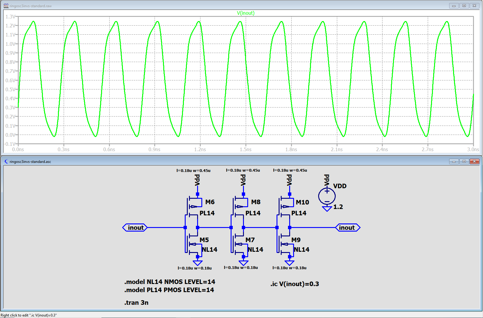
You can introduce device capacitances into consideration by specifying the model level parameter. Setting LEVEL=14, like in a statement '.model NL14 NMOS LEVEL=14' below, gives you the BSIM4.6.1 model:

3inv-osc

The other directives to notice are '.ic V(inout)=0.3' -- without this directive the oscillation start is delayed; and length/width parameters of the transistors. To bring MOSFET length/width parameter to the screen, right-click on the device symbol with ctrl key pressed and mark the Vis field. The parameter values are in the field 'Value2'.

You can experiment with different model level parameter values, like 9 or 12 -- see LTspice help, only do not forget to read messages appearing in the SPICE Error Log.

\$\endgroup\$
5
  • \$\begingroup\$ thank you. I was able to get the oscillation to start but I have a doubt about the shape of the waveform. I noticed that it is shaped like a sinusoid but in some cases the square shape is retained. Do you know what changes the shape of the waveform from a sin to a square? \$\endgroup\$ Commented Dec 4, 2023 at 0:46
  • 1
    \$\begingroup\$ @spiderman19 It may not be easily seen, but another thing the simulation in this answer does differently is it properly connects all the MOSFET pins. In your schematic screenshots the nmos4 and pmos4 symbols are connected incorrectly. Your body nodes are all floating. It's difficult to see because the dark blue and light blue look so similar but it's there. Pull up the SPICE error log (CTRL+L) post-simulation to confirm. Either draw it like in this answer or any other way where you don't get a floating node warning in the log. In general, avoid going "through" dark blue lines. \$\endgroup\$
    – Ste Kulov
    Commented Dec 4, 2023 at 4:02
  • 1
    \$\begingroup\$ The MOSFET ring oscillator is not a weapon of choice to generate a periodic waveform free of higher harmonics; it cannot and, in fact, never does generate either a pure sine wave or a pure square wave. The generated waveform is shaped by a complex interplay of the CMOS inverter's voltage transfer curve and non-linear MOSFET capacitances. \$\endgroup\$
    – V.V.T
    Commented Dec 4, 2023 at 14:31
  • 1
    \$\begingroup\$ Unlike, say, the case of Wien bridge oscillator, there exist no compact formulas suitable to describe the MOSFET ring oscillator behavior -- simply because the Wien bridge oscillator is basically a quasi-linear circuit with a small non-linearity introduced to provide automatic gain control, whereas the MOSFET ring oscillator is essentially a non-linear circuit. \$\endgroup\$
    – V.V.T
    Commented Dec 4, 2023 at 14:31
  • 1
    \$\begingroup\$ You can use simulations to build up your intuition. Examine CMOS inverters: how the inverter's VTC depends on NMOS/PMOS sizing and what are the resulting waveform shapes; run tran analysis simulations with a large-signal sine wave fed to the inverter input and how the output signal changes with frequency, etc (small signal analysis is of little use here). The plots you receive in this simulations are worth a million words. \$\endgroup\$
    – V.V.T
    Commented Dec 4, 2023 at 14:32

Your Answer

By clicking “Post Your Answer”, you agree to our terms of service and acknowledge you have read our privacy policy.

Not the answer you're looking for? Browse other questions tagged or ask your own question.