The bi-directional logic level shifter is not meant to drive load(s) on either or both sides. It is used for signaling or data communication between the low-side (LV) and the high-side (HV).
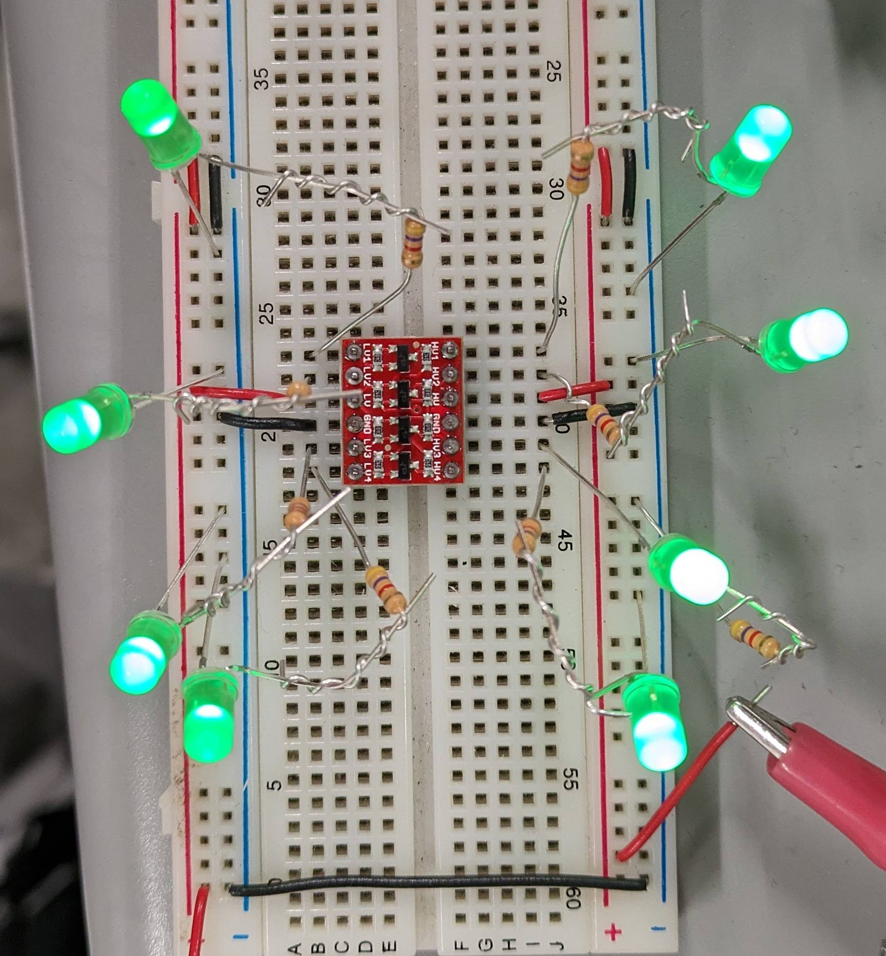
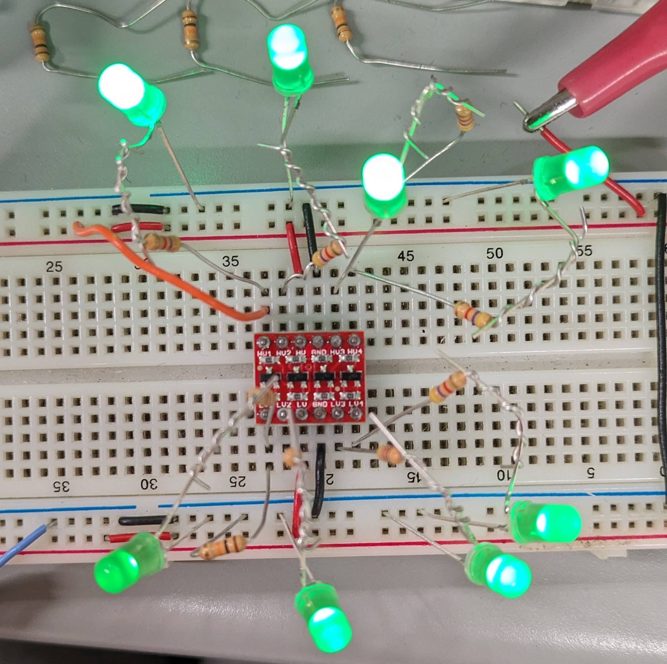
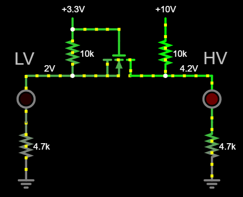
By connecting loads (each with a 4.7kΩ resistor and an LED) on both sides you get voltage dividers on LV and HV like the following example

Notice that LV is 2V and HV is 4.2V, which are calculable, and they are not floating. This is not how it is supposed to be used.
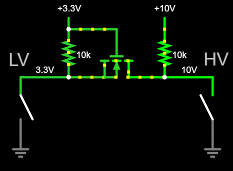
The voltage level shifter is only suitable for communicating devices that have open-drain output driver, meaning the connected devices should only pull (sink current) but not push (source current). Here is an example

The circuit uses switches in place of open-drain output drivers. By closing the switch (imitating sinking current to GND) on the LV side only, you will see the LV voltage drops to 0V and the HV will drop very close to 0V too. Similar effect will happen if you close the switch on the HV side only or both sides. Otherwise both sides will be pulled up to their respective power supply voltages (3.3V and 10V in this case like the figure above).
Internally the outputs are pulled high by 10k's, and I have seen many examples online of no pulldowns used.
Of course you can't find one because it is not meant to be used that way.
Edited Again
If your purpose is to send data from HV to LV and the transmitter's output driver is a push-pull type, you can use the Bi-directional Logic Level Shifter, provided that it must be a unidirectional communication.
Here is the circuit where the receiver is on the LV side and the transmitter is on the HV side.

You can push and pull by clicking on the SPDT switch on the HV side, imitating a push-pull output driver. I removed the pull-up resistor on the HV side because it is not needed (but no harm if it remains). I added a 100Ω resistor on the LV side to prevent voltage spikes from damaging the MCU's receiving pin when the transmitter switches between 0V and 10V. The transients are due to fast switching that get coupled from the HV side to the LV side through the MOSFET parasitic capacitance.
Here is the result
| HV side (transmitter with push-pull output driver) |
LV side (receiver) |
| 10V |
3.3V |
| 0V |
~0V |
Here is the circuit where the transmitter is on the LV side and the receiver is on the HV side.

There is no need for the 100Ω transient suppressing resistor because it will not do any harm to the circuit on the HV side.
Here is the result
| LV side (transmitter with push-pull output driver) |
HV side (receiver) |
| 3.3V |
10V |
| 0V |
~0V |

