0
\$\begingroup\$

I want generate a 5 volt, around 55 Hz(50-60) square wave with an NE555S-13.

In the datasheet, I found the configuration for astable operation which I assume is what I want:
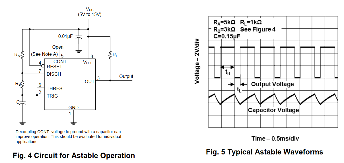
enter image description here screenshot from datasheet: https://www.diodes.com/assets/Datasheets/NE555_SA555_NA555.pdf

I found that the NE555S-13 is featured in the Falstad web simulator.

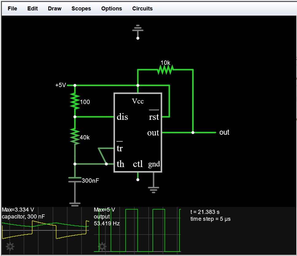
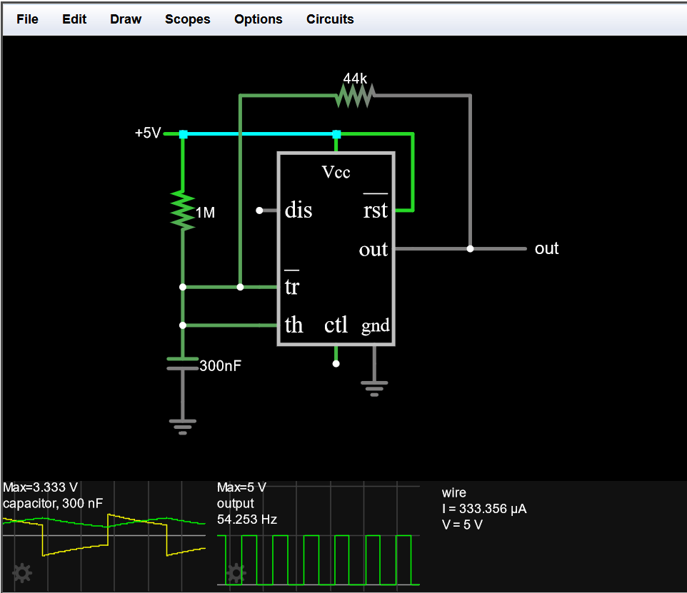
The problem is that in Falstad, the configuration for square generation is different and I don't know what to make of it, the main difference I see is that the "output" is pulled up to 5 volts at the Vcc pin in the datasheet's example while in the Falstad simulation it's pulled up at the trigger pin.

Is there some significant difference because when I simulated both configurations I saw seemingly similar results in the wave generation.

Is there something I am not seeing?

enter image description here

enter image description here

\$\endgroup\$
1
  • 1
    \$\begingroup\$ Hi, George. Take a good close look at the circuits. Trace the connections. You'll find that they are, in fact, almost identical electrically. Review the circuits, find the real differences (there's at least one,) then ask a direct question about the differences you find. \$\endgroup\$
    – JRE
    Commented Jun 11 at 10:46

1 Answer 1

2
\$\begingroup\$

The 555 output stage is not symmetrical. That is, it does not pull the output up as close to Vcc as it pulls the output down to GND. The datasheet has the real numbers, but IIRC it is something like the high output voltage is Vcc-1.5 V, while the low output voltage is 0.5 V (above GND).

In the first schematic, the resistor from Out to Vcc helps pull the output up a little higher. This usually is not a problem, but some downstream circuits need a more symmetrical output than others. The added resistor does not affect the frequency or duty cycle calculations.

The second schematic is a bit different. Its performance is different for the CMOS 555 compared to the bipolar 555. Basically, the intent is to produce a true 50/50 squarewave, something the standard astable circuit for the bipolar 555 has a problem with. The second schematic is the first time I've seen the circuit with the added 1 M resistor, and it will have a small effect on the output frequency. Again, it is there to compensate for the asymmetrical nature of the bipolar 555 output. The CMOS 555 has an almost perfectly symmetrical output stage, and should not need the added 1 M resistor.

If you have any questions, I can expand on this later today.

\$\endgroup\$

Your Answer

By clicking “Post Your Answer”, you agree to our terms of service and acknowledge you have read our privacy policy.

Not the answer you're looking for? Browse other questions tagged or ask your own question.