While playing around with the Howland current source in a simulator, I produced a simple multi-range configuration I've not seen published before, and haven't been able to find with an (albeit brief) search on the net. Can anybody point to a publication of this configuration?
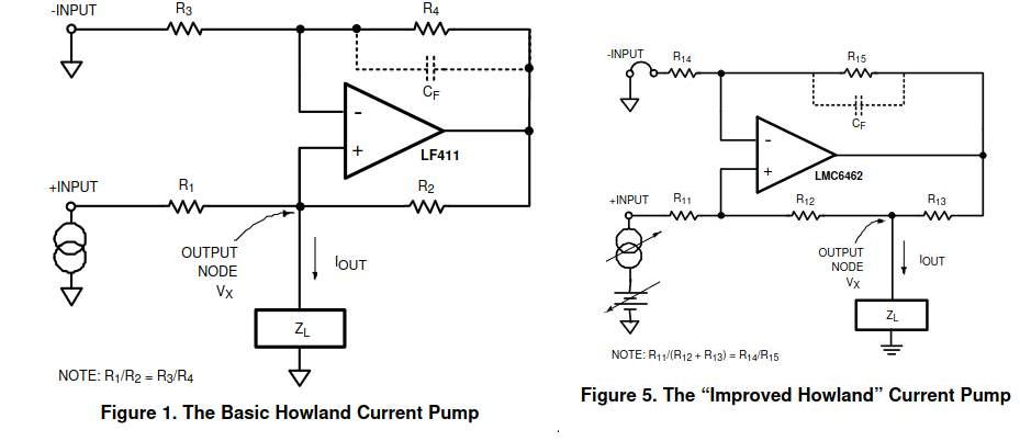
The classic application note from TI AN1515 / snoa474 shows the classic version, and an 'improved' version with a higher output current and a reduced need for excess headroom from the amplifier. Schematics from that paper.
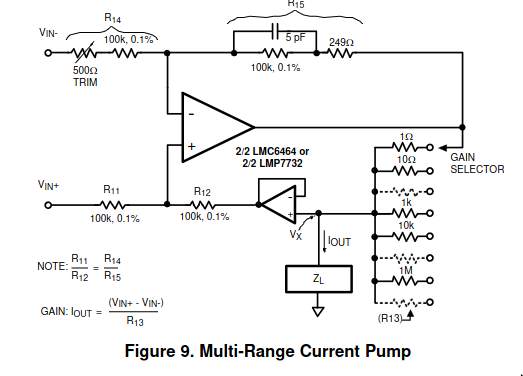
The progression from one diagram to the next suggested a possible configuration where the R12/R13s were switchable in the second diagram to get a multiple range output. However, looking in the TI paper, the only suggestion for multiple output ranges was the following, which is a totally different configuration.
The circuit does have the benefit that it is intuitively obvious how the range change is achieved, and that the basic differential amplifier on the left, being buffered from the range resistors, is always balanced and so delivers a theoretical infinite output impedance. However, it uses an extra gain block, and I'm always reluctant to put extra voltage offsets and delays into an amplifier's feedback path, quite apart from the aesthetics of a smaller solution. I will note that while the switches need to be perfect in this this layout, a straightforward '4-terminal type' rearrangement of the resistors and switches will take them out of the voltage path.
I played with the Fig 5 version in LTSPICE. To measure the output impedance, I swept the voltage at the output node with a voltage source, measuring the current through the same voltage source. Ideally it would be constant.
The AN1515 paper does state that it's the ratio (R12+R13)/R11 that has to match R15/R14, and indeed the simulation bore this out. However, the paper doesn't make the intuitive leap that occurred to me, that as R12+R13 is constant, you are just tapping off from some point along it. You could use more resistors than two, to have a wider range of current outputs.
The key observation is that, if we refer to Fig 1's R2, or fig 5's R12+R13, or my R4,5,6,7 as the 'output resistor', then tapping at Any Point on the output resistor yields an infinite impedance current source output, with different gm at different points.
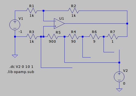
This is what I simulated (changing the output wire between runs, rather than implementing switches).
Taking the output current from one of the four positions shown gives decade ranges, each with infinite output impedance (for infinite gain op-amp and ideal component values). As the selection switches are in series with a high impedance, they can be any type of switch, with a high or even non-linear resistance, so even BJT's.
I've attached the .asc file, if you want to play with it, and see the effect of finite amplifier gain or resistor mismatch on output impedance.
I've not seen this before, have you?
Version 4
SHEET 1 880 680
WIRE 0 64 -64 64
WIRE 112 64 80 64
WIRE 256 64 112 64
WIRE 624 64 336 64
WIRE -64 112 -64 64
WIRE 112 128 112 64
WIRE 176 128 112 128
WIRE 624 144 624 64
WIRE 624 144 240 144
WIRE 176 160 112 160
WIRE -64 224 -64 192
WIRE 0 224 -64 224
WIRE 96 224 80 224
WIRE 112 224 112 160
WIRE 112 224 96 224
WIRE 128 224 112 224
WIRE 240 224 208 224
WIRE 256 224 240 224
WIRE 352 224 336 224
WIRE 384 224 352 224
WIRE 480 224 464 224
WIRE 496 224 480 224
WIRE 624 224 624 144
WIRE 624 224 576 224
WIRE 480 320 480 224
WIRE 544 320 480 320
WIRE -64 336 -64 224
WIRE 352 352 352 224
WIRE 400 352 352 352
WIRE 240 384 240 224
WIRE 576 384 576 304
WIRE 576 384 240 384
WIRE 96 416 96 224
WIRE 288 416 96 416
WIRE 576 432 576 384
WIRE 576 544 576 512
FLAG -64 336 0
FLAG 576 544 0
SYMBOL OpAmps\\opamp 208 80 R0
SYMATTR InstName U1
SYMATTR SpiceLine Aol=100Meg
SYMBOL res 96 48 R90
WINDOW 0 0 56 VBottom 2
WINDOW 3 32 56 VTop 2
SYMATTR InstName R1
SYMATTR Value 1k
SYMBOL res 352 48 R90
WINDOW 0 0 56 VBottom 2
WINDOW 3 32 56 VTop 2
SYMATTR InstName R2
SYMATTR Value 1k
SYMBOL res 96 208 R90
WINDOW 0 0 56 VBottom 2
WINDOW 3 32 56 VTop 2
SYMATTR InstName R3
SYMATTR Value 1k
SYMBOL res 352 208 R90
WINDOW 0 0 56 VBottom 2
WINDOW 3 32 56 VTop 2
SYMATTR InstName R4
SYMATTR Value 90
SYMBOL voltage -64 96 R0
WINDOW 123 0 0 Left 0
WINDOW 39 0 0 Left 0
SYMATTR InstName V1
SYMATTR Value -1
SYMBOL voltage 576 416 R0
WINDOW 123 0 0 Left 0
WINDOW 39 0 0 Left 0
SYMATTR InstName V2
SYMATTR Value 0
SYMBOL res 224 208 R90
WINDOW 0 2 21 VBottom 2
WINDOW 3 32 56 VTop 2
SYMATTR InstName R5
SYMATTR Value 900
SYMBOL res 480 208 R90
WINDOW 0 0 56 VBottom 2
WINDOW 3 32 56 VTop 2
SYMATTR InstName R6
SYMATTR Value 9
SYMBOL res 592 208 R90
WINDOW 0 0 56 VBottom 2
WINDOW 3 32 56 VTop 2
SYMATTR InstName R7
SYMATTR Value 1
TEXT -112 440 Left 2 !.lib opamp.sub
TEXT -96 408 Left 2 !.dc V2 0 10 1


