2
\$\begingroup\$

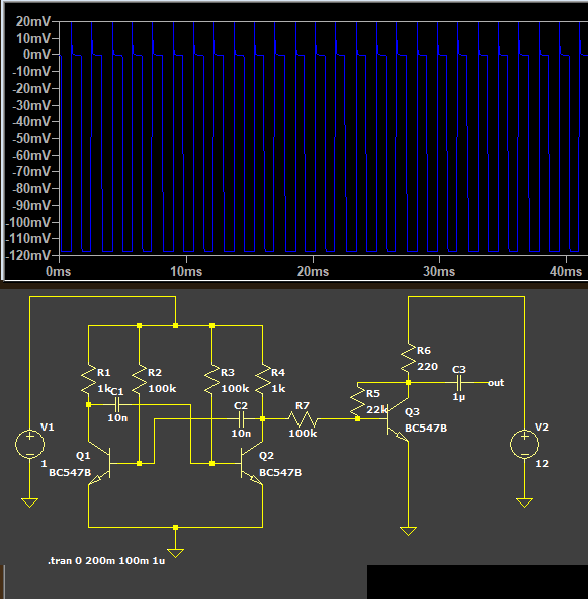
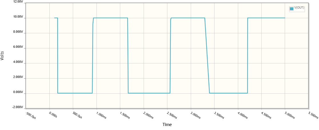
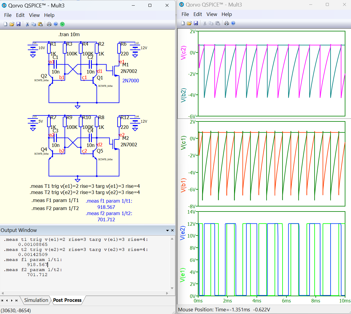
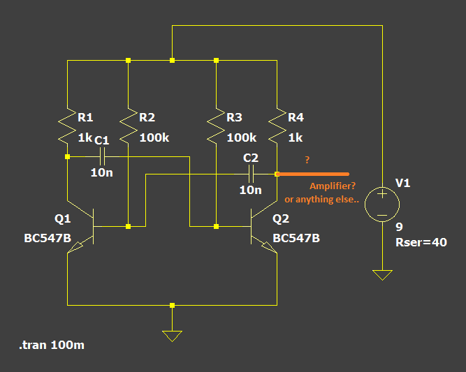
I managed to develop an astable multivibrator transistor square wave generator of ~710Hz. This generator will be used as sound for AM radio transmission. The sound must be amplified by an external circuit. The simulation and realization of the generator works fine, but when I want to snatch voltage from this generator at a certain point, it is getting unstable.

I tried putting a capacitor across the voltage source for impedance matching and I could still not figure out why I could not make it work. I don't suppose the failure was just that. Below a picture of the circuit.

How can I extend a basic circuit in conjunction with another one without having to many disadvantages?

circuit

Edit:

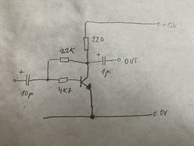
As demanded below an example:

preamp

Edit2:

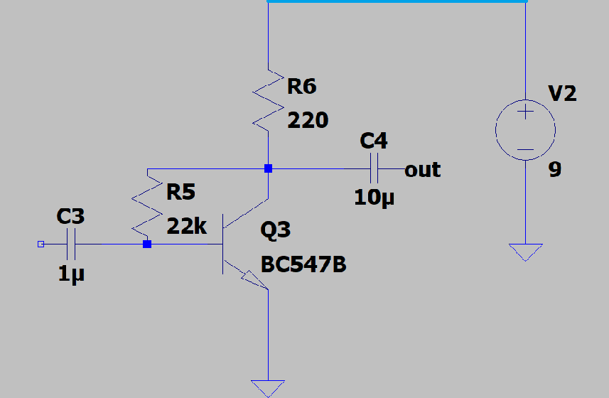
The amplifier right from the square generator has the following example components: (The values can vary, I just tried with few ones, but had no luck.)

preamp

Edit3:

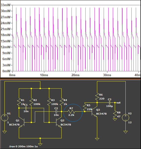
I succeeded to make the circuits working together. I added a 100kohm resistor to the output of oscillator, but it suffered this time from less gain. Why did I do this? I intended to get a good signal output from the oscillator without changing its appearance and further to amplify it. I think I need a multistage amplification method.

Here the circuit:

loadv2

The .asc file of LTspice:

Version 4
SHEET 1 1560 680
WIRE 256 -144 -64 -144
WIRE 1024 -144 768 -144
WIRE 176 -80 64 -80
WIRE 256 -80 256 -144
WIRE 256 -80 176 -80
WIRE 336 -80 256 -80
WIRE 448 -80 336 -80
WIRE 768 -48 768 -144
WIRE 64 0 64 -80
WIRE 176 0 176 -80
WIRE 336 0 336 -80
WIRE 448 0 448 -80
WIRE 768 48 768 32
WIRE 768 48 656 48
WIRE 848 48 768 48
WIRE 944 48 912 48
WIRE 768 80 768 48
WIRE 64 96 64 80
WIRE 96 96 64 96
WIRE 288 96 160 96
WIRE 368 128 208 128
WIRE 448 128 448 80
WIRE 448 128 432 128
WIRE 496 128 448 128
WIRE 656 128 576 128
WIRE 704 128 656 128
WIRE -64 144 -64 -144
WIRE 1024 144 1024 -144
WIRE 64 176 64 96
WIRE 448 176 448 128
WIRE 176 224 176 80
WIRE 176 224 128 224
WIRE 208 224 208 128
WIRE 208 224 176 224
WIRE 288 224 288 96
WIRE 336 224 336 80
WIRE 336 224 288 224
WIRE 384 224 336 224
WIRE -64 304 -64 224
WIRE 1024 304 1024 224
WIRE 64 368 64 272
WIRE 256 368 64 368
WIRE 448 368 448 272
WIRE 448 368 256 368
WIRE 768 368 768 176
WIRE 256 416 256 368
FLAG -64 304 0
FLAG 256 416 0
FLAG 944 48 out
FLAG 1024 304 0
FLAG 768 368 0
SYMBOL npn 128 176 M0
SYMATTR InstName Q1
SYMATTR Value BC547B
SYMBOL npn 384 176 R0
SYMATTR InstName Q2
SYMATTR Value BC547B
SYMBOL res 48 -16 R0
SYMATTR InstName R1
SYMATTR Value 1k
SYMBOL res 160 -16 R0
SYMATTR InstName R2
SYMATTR Value 100k
SYMBOL res 320 -16 R0
SYMATTR InstName R3
SYMATTR Value 100k
SYMBOL res 432 -16 R0
SYMATTR InstName R4
SYMATTR Value 1k
SYMBOL voltage -64 128 R0
WINDOW 123 0 0 Left 0
WINDOW 39 24 124 Left 2
SYMATTR InstName V1
SYMATTR Value 1
SYMBOL cap 160 80 R90
WINDOW 0 0 32 VBottom 2
WINDOW 3 32 32 VTop 2
SYMATTR InstName C1
SYMATTR Value 10n
SYMBOL cap 432 112 R90
WINDOW 0 0 32 VBottom 2
WINDOW 3 32 32 VTop 2
SYMATTR InstName C2
SYMATTR Value 10n
SYMBOL res 640 32 R0
SYMATTR InstName R5
SYMATTR Value 22k
SYMBOL res 752 -64 R0
SYMATTR InstName R6
SYMATTR Value 220
SYMBOL npn 704 80 R0
SYMATTR InstName Q3
SYMATTR Value BC547B
SYMBOL voltage 1024 128 R0
WINDOW 123 0 0 Left 0
WINDOW 39 24 124 Left 2
SYMATTR InstName V2
SYMATTR Value 12
SYMBOL res 592 112 R90
WINDOW 0 0 56 VBottom 2
WINDOW 3 32 56 VTop 2
SYMATTR InstName R7
SYMATTR Value 100k
SYMBOL cap 912 32 R90
WINDOW 0 0 32 VBottom 2
WINDOW 3 32 32 VTop 2
SYMATTR InstName C3
SYMATTR Value 1µ
TEXT -24 440 Left 2 !.tran 0 200m 100m 1u

\$\endgroup\$
7
  • \$\begingroup\$ Can you put a picture of your setup as well? but when I want to snatch voltage from this generator at a certain point what do you mean by that? Probing or applying to a load or something else? Finally, why does your power source has 40 Ohms of output impedance? \$\endgroup\$ Commented Aug 12 at 11:17
  • \$\begingroup\$ @RohatKılıç I edited my question. I hope it will help more. TY. Can you tell me why the Rser=40ohm has an issue with the question? I need it for current limitation. If I am wrong, please inform me. 'm just newbie. \$\endgroup\$ Commented Aug 12 at 11:27
  • \$\begingroup\$ 40 Ohms of output impedance for a power supply is unusual, unless it's some sort of signal generator. Anyway. You didn't put the photo of the setup. It'd help to see why it was going unstable. By the way, have you considered using an op amp instead? Today you can find ICs with two independent op amps, so one can be used for the oscillator and the other for the amplifier. \$\endgroup\$ Commented Aug 12 at 11:42
  • \$\begingroup\$ @RohatKılıç TY for your suggestions. But I complain about the understanding, how to bring two independent circuits working together and yes, I will reconsider the op amps in the future. \$\endgroup\$ Commented Aug 12 at 11:56
  • \$\begingroup\$ Fundamentally, there's no problem with cascading the two blocks shown in the question. The key here is to have the amplifier's input impedance higher enough than the oscillator's output impedance. Otherwise the amplifier will load the oscillator and it'll lose the balance therefore go unstable. Please, if you can, show us a photo of the setup (i.e. physical circuit and how it's hooked up), it'll help a lot. Sometimes the biggest problem can be the breadboard or bad soldering or wiring. \$\endgroup\$ Commented Aug 12 at 12:11

4 Answers 4

2
\$\begingroup\$

Short answer

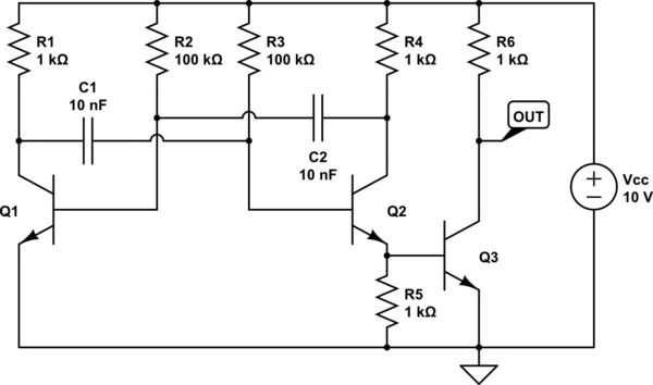
You can resolve the matching problem between the two devices by cascading Q2 and Q3 transistors. To do this, you can insert the base-emitter junction of Q3 into the emitter circuit of Q2.

Understanding vs knowing

Since you seem really curious about this circuit, I thought I would share some of my tricks for getting a real grasp of these basic transistor circuits. Instead of just memorizing stuff from textbooks, I like to use my intuition and imagination. That is the key to truly understanding a circuit, not just knowing the facts.

Where is the transistor output?

To answer this question, we need a functional understanding of the transistor, i.e., what it does and how it does it in a general sense. In essence, we need to conceptualize it as a functional block.

Current sink

If we look into the collector of a transistor, we will see the current disappearing into it as if it were some kind of "black hole". We then say that an (NPN) transistor is a “current sink” that absorbs current. To convert it to voltage, we should connect a collector resistor in series and take the voltage drop across it as an output. The problem is that this voltage is not referenced to ground. So, we take its complement - the collector-emitter voltage, as an output connecting a high-resistance load in parallel to the collector-emitter part. That is why this output is inverted.

Current source

If we look into the emitter, we will see the current flowing out of it. We then say that the transistor is a “current source” that produces current. We can take the emitter current as an output quantity by connecting a low-resistance load in series.

Both current sink and source

Finally, we can use a transistor both as a current sink and source. The current entering the collector and exiting the emitter is (almost) the same, and is determined by the instantaneous conductance of the collector-emitter region (we can imagine it as a variable resistor that changes its resistance).

So, a BJT has two output terminals - collector and emitter, and we can use one, the other, or both as outputs.

Where is the OP's circuit output?

Now let's apply the observations above to OP's circuit.

Collector output

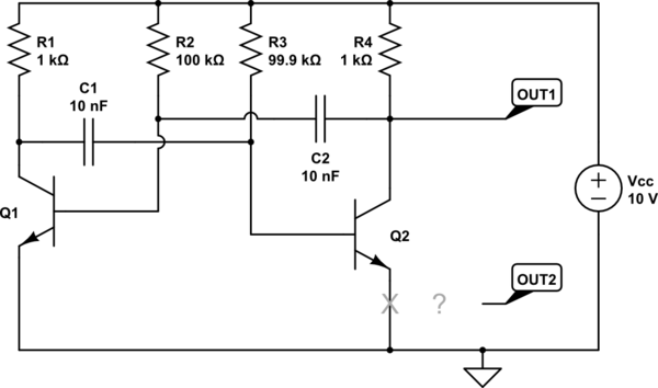
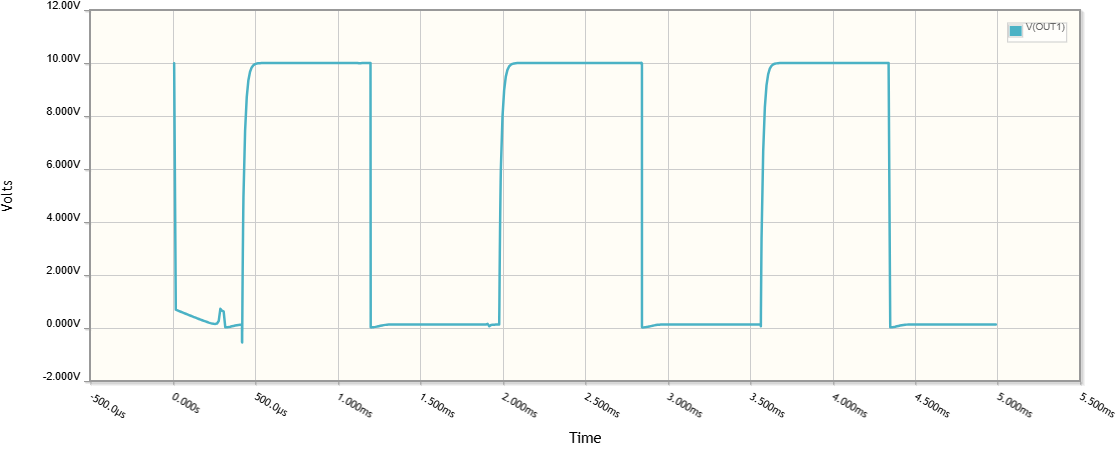
If the load is high-resistance enough, we can connect it in parallel to Q2's collector-emitter part (OUT1). However, a BJT has a low-resistance input (base-emitter junction). So, to connect it to the high-resistance Q2's output, we can insert a base resistor. Then the next stage will act as a transistor switch.

schematic

simulate this circuit – Schematic created using CircuitLab

This is not an analog circuit (amplifier) because the transistor operates in both of its extreme states - on and off. Actually, since the collector voltage changes from the minimum to the maximum supply voltage, there is no need for an amplifier; a simple emitter follower can serve as a buffer.

STEP 1

The requirement for a high load resistance stems from the fact that the collector resistor and the load form a voltage divider, causing the output voltage to decrease. This also affects the operation of the circuit itself (charging the capacitor C2).

Emitter output

If the load is low-resistance, we can connect it in series to Q2's collector-emitter part, from the emitter side (OUT2). In the OP's case, the BJT has a low-resistance input (base-emitter junction). So, to connect it in series to Q2's emitter output (OUT2), we do not need a resistor. Q2's input serves as a current load inserted in the loop.

schematic

simulate this circuit

STEP 2

Directly connecting transistors in this manner creates a configuration known as a "cascode".

\$\endgroup\$
2
\$\begingroup\$

You can try to add some base resistor to amp so it increases the amp input impedance.

enter image description here

\$\endgroup\$
1
\$\begingroup\$

The problem was about connecting two independent circuits. One circuit is an oscillator and the other one is just an amplifier. While connecting them, the way is keeping the input impedance of the amplifier higher than the output impedance of the oscillator. Otherwise, the circuits will unbalance and the output will be unstable.

solution

.asc file "ltspice"

Version 4
SHEET 1 1560 680
WIRE 256 -144 -64 -144
WIRE 1024 -144 768 -144
WIRE 176 -80 64 -80
WIRE 256 -80 256 -144
WIRE 256 -80 176 -80
WIRE 336 -80 256 -80
WIRE 448 -80 336 -80
WIRE 768 -48 768 -144
WIRE 64 0 64 -80
WIRE 176 0 176 -80
WIRE 336 0 336 -80
WIRE 448 0 448 -80
WIRE 768 48 768 32
WIRE 768 48 656 48
WIRE 848 48 768 48
WIRE 928 48 912 48
WIRE 944 48 928 48
WIRE 768 80 768 48
WIRE 64 96 64 80
WIRE 96 96 64 96
WIRE 288 96 160 96
WIRE 928 112 928 48
WIRE 368 128 208 128
WIRE 448 128 448 80
WIRE 448 128 432 128
WIRE 496 128 448 128
WIRE 656 128 576 128
WIRE 704 128 656 128
WIRE -64 144 -64 -144
WIRE 1024 144 1024 -144
WIRE 64 176 64 96
WIRE 448 176 448 128
WIRE 176 224 176 80
WIRE 176 224 128 224
WIRE 208 224 208 128
WIRE 208 224 176 224
WIRE 288 224 288 96
WIRE 336 224 336 80
WIRE 336 224 288 224
WIRE 384 224 336 224
WIRE -64 304 -64 224
WIRE 1024 304 1024 224
WIRE 64 368 64 272
WIRE 256 368 64 368
WIRE 448 368 448 272
WIRE 448 368 256 368
WIRE 768 368 768 176
WIRE 256 416 256 368
FLAG -64 304 0
FLAG 256 416 0
FLAG 944 48 out
FLAG 1024 304 0
FLAG 768 368 0
FLAG 928 192 0
SYMBOL npn 128 176 M0
SYMATTR InstName Q1
SYMATTR Value BC547B
SYMBOL npn 384 176 R0
SYMATTR InstName Q2
SYMATTR Value BC547B
SYMBOL res 48 -16 R0
SYMATTR InstName R1
SYMATTR Value 1k
SYMBOL res 160 -16 R0
SYMATTR InstName R2
SYMATTR Value 100k
SYMBOL res 320 -16 R0
SYMATTR InstName R3
SYMATTR Value 100k
SYMBOL res 432 -16 R0
SYMATTR InstName R4
SYMATTR Value 1k
SYMBOL voltage -64 128 R0
WINDOW 123 0 0 Left 0
WINDOW 39 24 124 Left 2
SYMATTR InstName V1
SYMATTR Value 1
SYMBOL cap 160 80 R90
WINDOW 0 0 32 VBottom 2
WINDOW 3 32 32 VTop 2
SYMATTR InstName C1
SYMATTR Value 10n
SYMBOL cap 432 112 R90
WINDOW 0 0 32 VBottom 2
WINDOW 3 32 32 VTop 2
SYMATTR InstName C2
SYMATTR Value 10n
SYMBOL res 640 32 R0
SYMATTR InstName R5
SYMATTR Value 22k
SYMBOL res 752 -64 R0
SYMATTR InstName R6
SYMATTR Value 220
SYMBOL npn 704 80 R0
SYMATTR InstName Q3
SYMATTR Value BC547B
SYMBOL voltage 1024 128 R0
WINDOW 123 0 0 Left 0
WINDOW 39 24 124 Left 2
SYMATTR InstName V2
SYMATTR Value 12
SYMBOL res 592 112 R90
WINDOW 0 0 56 VBottom 2
WINDOW 3 32 56 VTop 2
SYMATTR InstName R7
SYMATTR Value 2.2k
SYMBOL cap 912 32 R90
WINDOW 0 0 32 VBottom 2
WINDOW 3 32 32 VTop 2
SYMATTR InstName C3
SYMATTR Value 100µ
SYMBOL res 912 96 R0
SYMATTR InstName R8
SYMATTR Value 47
TEXT -24 440 Left 2 !.tran 0 200m 100m 1u

\$\endgroup\$
2
  • 4
    \$\begingroup\$ The input impedance of the second stage needs to be not just just "higher" than the first stage output impedance, but significantly higher, if you want to ensure that the second stage doesn't significantly load the first stage. \$\endgroup\$
    – Hearth
    Commented Aug 12 at 14:25
  • \$\begingroup\$ proper, the idea of answering your own question deserves encouragement, not silence. I have a few comments on your answer: 1) You say that your second stage is an amplifier, but in fact it reduces the output voltage of the multivibrator. And in general, do you need a (voltage) amplifier? 2) It would be good if the graphical representation showed several periods of the signal. To do this, you should decrease the simulation time. \$\endgroup\$ Commented Aug 15 at 15:55
1
\$\begingroup\$

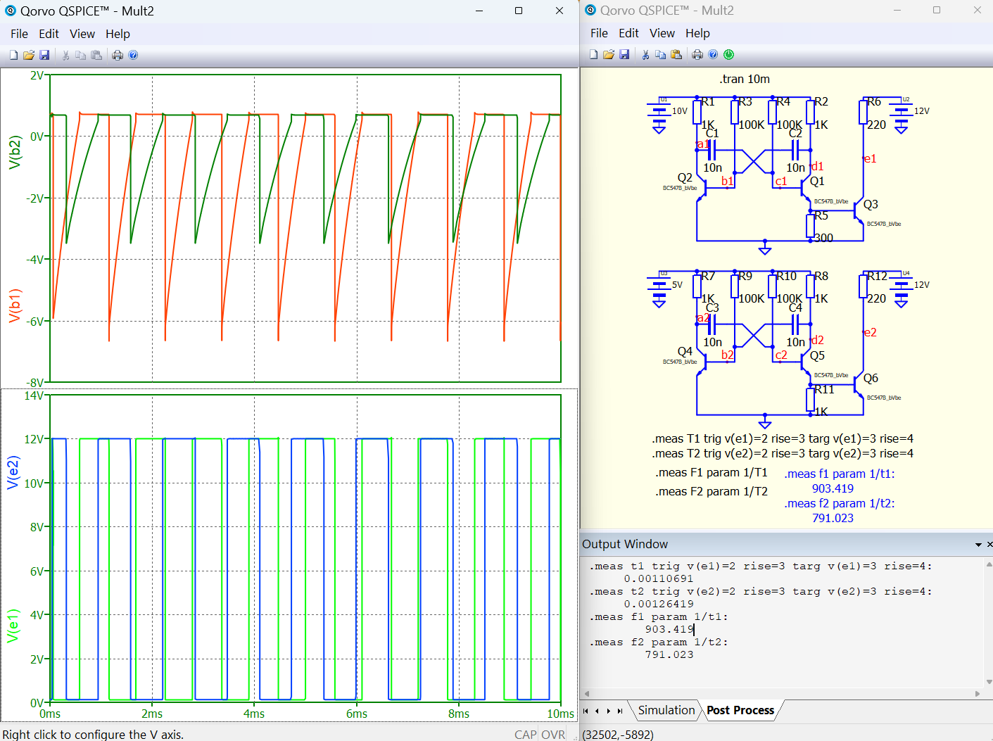
At a supply voltage of 9 V, harmful effects such as emitter junction breakdown already appear. In addition to the fact that the transistors slowly degrade (BETA current gain drops), the frequency is higher. I added to the model a Base-Emitter breakdown of 6V at 10µA current. You can do this in LTspice as well. See what you get: enter image description here

enter image description here

\$\endgroup\$

Your Answer

By clicking “Post Your Answer”, you agree to our terms of service and acknowledge you have read our privacy policy.

Not the answer you're looking for? Browse other questions tagged or ask your own question.