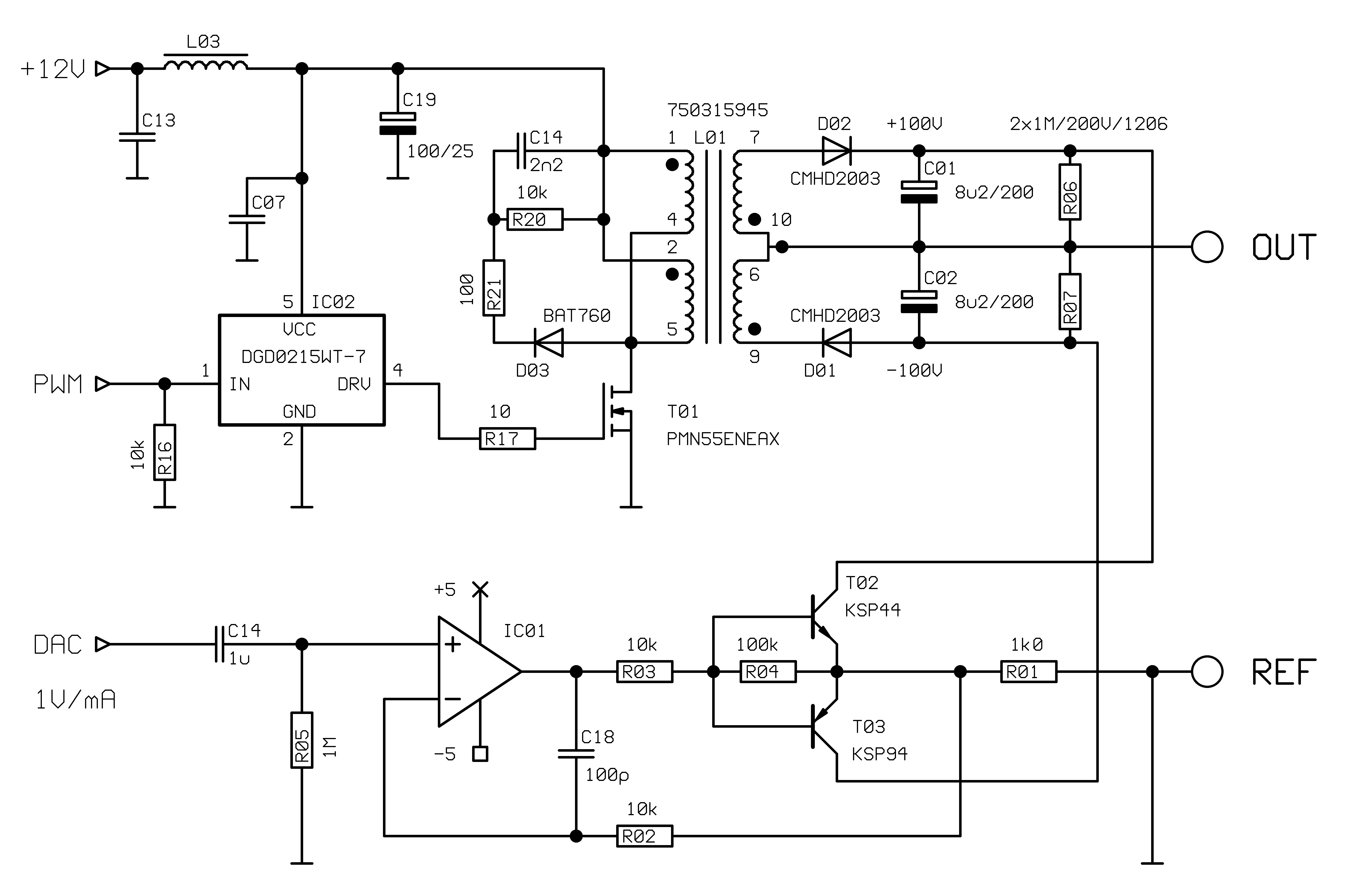
I'm trying to design a neuro-stimulator-like circuit around an ESP32-S3. The output needs to be bipolar / biphasic (it's floating so an H-bridge will do), current limited, and the current needs to be controllable from the ESP32, likely with a digipot or DAC. The ESP32 is likely too slow to be in the control loop, but is fast enough to generate the 4 signals for the H-bridge.
Let me preface this by saying that the parameters I want to achieve are:
- a train of 3 biphasic pulses (plus-minus x 3, with 1 ms of pause in between) at most once a second - means the average power is extremely low
- pulse length 50-150 µs per phase (if it's 50 µs, we can say the frequency is 20 kHz)
- current limited to 1-10 mA, adjustable by the microcontroller, with max voltage of 120 V into a load of 10-100 kΩ
I have several ideas on how to achieve this, but they all seem to be a bit overkill, so I'm turning to you for solutions on how to simplify this circuit. It's for an open-source project that needs to be as cheap and as small as possible (fewer components = better).
I also have a working prototype that creates the required waveform with a bootstrapped improved Howland current pump, which is extremely overkill - it has a lot of components and requires a bipolar power supply (so 2 flyback transformers or a 2-secondary one). Moreover, I don't neet to generate arbitrary current waveforms, I just need short bursts of current-limited pulses. Also, it uses many components, some of which are relatively expensive. I also don't benefit from having ± rails, because the output is floating anyway (a double-insulated, battery powered device).
So for the new design, what comes to mind is having a single HV power supply, an H-bridge for making bipolar (biphasic) pulses from that voltage, and some sort of a current-limiting circuit with an adjustable current.
For the PSU, what I currently have is a little SMD flyback transformer (Coilcraft LPR6235-253PMRC) run with a MOSFET, and the PWM @ 100 kHz is generated by the ESP32-S3. This generates some 120 V from the battery's 3.2 - 4.2 V and charges an electrolytic cap. I don't think this part can be improved much, save for a better snubber circuit.
I have a 3.3 V rail, an unregulated 3.2-4.2 battery voltage, and a 120 V from the flyback. If it's possible, I'd rather not add another SMPS converter for an intermediary rail.
For the actual current switching and limiting part, I want to use something like this:
https://oshwlab.com/pscdietrich/high-voltage-h-bridge
I'd likely use some NPNs that can handle the 120 V, same goes for the MOSFETs.
ESP32-S3's GPIO module allows changing the states of many pins in 1 clock cycle, so I can use it to generate the signals to drive the H-bridge (I'll add dead time between switches just in case).
An alternative would be using a chip like DRV8833 to drive the MOSFET H-bridge.
As for the current limiting part, this comes to mind:
https://www.ti.com/lit/ab/sboa174d/sboa174d.pdf?ts=1723924270977
I could use something like an INA240 with a small current sensing resistor on the low side, and its output could either drive a schmitt-trigger-input quad AND-gate that ANDs the h-bridge driving signals with the output of the H-Bridge signal. The reference voltage would be provided by a DAC5571.
Another solution would be to take the output of the INA240 and feed it into a MOSFET or BJT that supplies the power for the top side of the H-bridge.
This would likely work even if the MOSFET ends up in the ohmic region most of the time while actually switching on, or I use a BJT, because I only need 3 x 150 µs pulses (up-down) every 5 seconds at most, which means the average current and power is miniscule and the device is unlikely to overheat.
The third solution would be using this circuit, or a low-side equivalent, with a digipot for R2. I don't think that'd work right off the bat, the voltage across the digipot might not be too high, but it's likely that it's offset too high compared to the MCU voltage.

