0
\$\begingroup\$

I have started the book The Elements of Computing Systems. I am at the point where I am making an OR gate, although I'm not getting the proper results.

I am using one NAND and one NOT gate for my OR gate. It goes like this:

schematic

simulate this circuit – Schematic created using CircuitLab

Why will my NOT1 gate not reverse the digital signal? Why does the below example work, even though it seems like the same logic? Which fundamental rule of electricity am I unaware of that makes my first design non-functional?

schematic

simulate this circuit

\$\endgroup\$
2
  • 2
    \$\begingroup\$ The two circuits that you show do not produce the same logical function result. \$\endgroup\$ Commented Apr 22, 2014 at 9:55
  • 2
    \$\begingroup\$ When you say that the first circuit does not work you'll have to provide a lot more information as to just what "not working" really means. What type of result did you expect? Did you actually build and power up the circuit? What types of chips were used on the prototype? \$\endgroup\$ Commented Apr 22, 2014 at 10:00

3 Answers 3

10
\$\begingroup\$

This is down to Boolean algebra rather than electronics. We have for your initial circuit with inputs \$A\$ and \$B\$ and output \$Q\$:

$$Q=\overline{\overline{A\land B}}=A\land B$$

Where \$\land\$ represents AND and \$\overline{\cdot}\$ represents NOT. So in this case you have created an AND gate. For the second circuit we have (where \$\lor\$ represents OR):

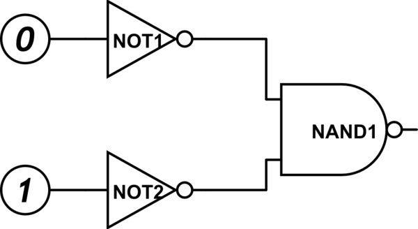
$$Q=\overline{\overline{A}\land\overline{B}}=A\lor B$$

By De-Morgan's laws. Therefore it is a functional OR gate.

Notice that the crucial difference between both of your expressions is the first one is negating the entirety of the NAND output whereas the second one negates each of the inputs before NANDing them.

\$\endgroup\$
1
  • \$\begingroup\$ The easy-to-remember rule is: slide the dots: if you pass through an and it becomes an or, and vice versa. And two dots cancel each other out. \$\endgroup\$ Commented Apr 22, 2014 at 11:24
1
\$\begingroup\$

A NAND gate functions internally as an AND gate followed by an inverter (indicated by the little circle at the right end). In your top example, you have a NAND gate followed by a second inverter, which simply turns the combination of the two gates into an AND gate -- not an OR gate at all.

The main thing to remember about a NAND gate, is if any input is 0, then the output is 1. (And the output is 0 only if both inputs are 1.)

So in the top example, the output of the NAND is 0 only if both inputs are 1, so the output of the explicit inverter is 1 only if both inputs of the NAND are 1 -- exactly as an AND gate should work.

In the bottom circuit, both inputs are inverted before being presented to the NAND gate. So now the rule becomes, if any input to the inverters is 1, then the output of the NAND gate is 1, and the output is 0 only if both inputs are 0. Gee, that's the definition of an OR gate.

If you haven't done so already, I would make up truth tables for a NAND gate by itself, and then two additional tables for the two circuits.

\$\endgroup\$
0
\$\begingroup\$

in Circuit1, NOT1 simply cancels the inverting in NAND1 giving the circuit the Boolean Expression NOT (NOT AND), that is, reading it from right to left , much like an assignment statement in software programming. it is actually ((AB)')' or, in another parlance, AB Bar-Bar, which is equal to just AB.

\$\endgroup\$

Your Answer

By clicking “Post Your Answer”, you agree to our terms of service and acknowledge you have read our privacy policy.

Not the answer you're looking for? Browse other questions tagged or ask your own question.