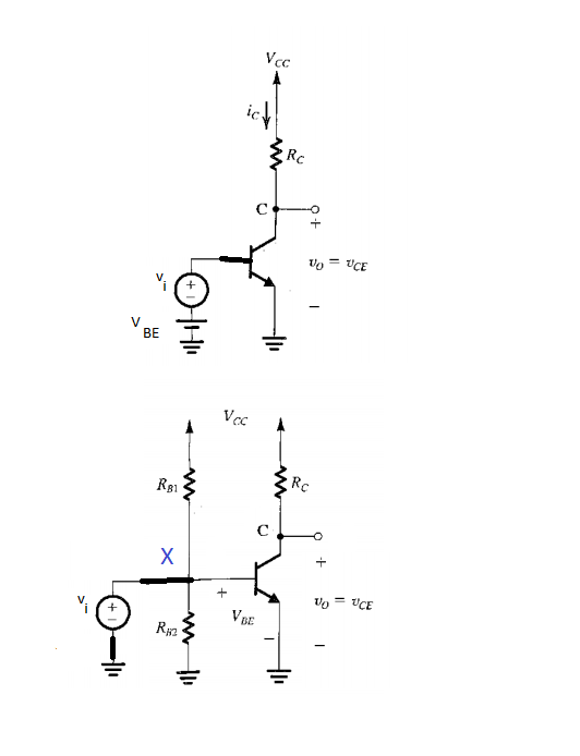
At the first fig. there is a basic common emitter amplifier circuit where signal source v_i is "superimposed" on the dc bias voltage V_BE. At the second fig. a biasing scheme (poor, nevertheless sufficient for my purpose) is shown where V_BE is fixed using a voltage divider across the power supply V_CC. Now, on numerous occasions, I have seen the signal source v_i is applied at node X (colored blue). Does this actually "superimpose" v_i on V_BE? How? Thanks.
-
\$\begingroup\$ Are the two figures equivalent? \$\endgroup\$– user40754Commented Apr 23, 2014 at 6:03
-
1\$\begingroup\$ The answer is in the part that I suspect you erased from the picture, the coupling capacitor. \$\endgroup\$– jippieCommented Apr 23, 2014 at 6:15
-
\$\begingroup\$ Without a coupling capacitor the resistor Rb2 will be shorted and there will be no proper dc biasing. \$\endgroup\$– LvWCommented Apr 23, 2014 at 6:47
-
\$\begingroup\$ Sorry, consider the coupling capacitor, I forgot. \$\endgroup\$– user40754Commented Apr 23, 2014 at 7:28
-
\$\begingroup\$ Now, if I add the coupling capacitor in the second one does that make the two figures equivalent? @LvW \$\endgroup\$– user40754Commented Apr 23, 2014 at 7:32
3 Answers
Question: Now, if I add the coupling capacitor in the second one does that make the two figures equivalent? @LvW
No - they are not. In the first circuit we have an IDEAL dc source (stiff), whereas in the 2nd circuit we have a voltage divider which delivers a voltage across a finite source resistance. As a consequence, the dc bias voltage at the base is not independent on the current into the base (which depends on the particular part and the temperature). However, because of practical reasons the 2nd circuit is, of course, used (with a current stabilizing resistor in the emitter path).
Question: Now, if I add the coupling capacitor in the second one does that make the two figures equivalent?
These two circuit are not equivalent. for the fig:1 , as you use a constant DC voltage source for biasing , these biasing voltage will be always same but no particular way to control base current Ib . But for fig:2 you can fix base voltage using voltage division rule and also using thevenin equivalent you can choose base current Ib . All you have to do , just choose RB1 and RB2 wisely.
Question: Does this actually "superimpose" v_i on V_BE yes.
For fig:1 , you just add two voltage source in series.Is there any reason not to be superimpose? I don't think so.
For fig:2 , if you consider the coupling capacitor then when you consider DC voltage, for DC voltage coupling capacitor act like open circuit. So you get a fixed voltage at node X . And then if you consider for V_i ( assuming it is small signal analysis ) then for small signal , coupling capacitor act like short circuit and so a voltages came from V_i . But from node X , the circuit only sense the equivalent circuit. So it sees a small change of it's fixed voltage which gives a situation like your fig:1 for voltage at node X. So it also superimposed.
But if signal from V_i is not that small then behavior of capacitor (impedance , open or short circuit etc ) depends its signals characteristics and make the calculation for the voltage at node X a little more clumsy. But This also superimpose .
-
\$\begingroup\$ For fig.2 When dc is considered the coupling capacitor makes v_i inactive. So, the circuit produces bias current I_C. When ac is considered V_CC is deactivated. So, the circuit produces signal current i_C. These two I_C and i_C according to superposition produces net current I_C+i_c. Is that correct? \$\endgroup\$ Commented Apr 23, 2014 at 12:51
-
\$\begingroup\$ yes. and as i_c is small it did not very Q point significantly. \$\endgroup\$– AnklonCommented Apr 23, 2014 at 15:23