23
\$\begingroup\$

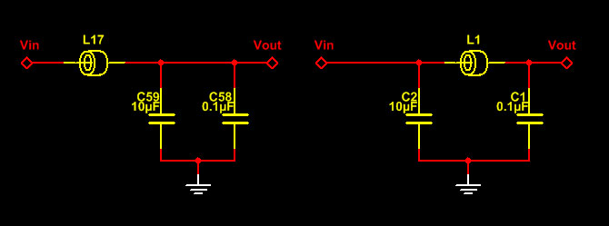
I wish to use some extra power supply filtering for my DAC, ADC, CPLD and OpAmp devices. In this question I got the point about the global locations for ferrite beads. If I understood correctly, the ferrite bead should be placed close to the device regardless whether it is a noise-generating, or noise-susceptible device. Please, correct me if it's not a general case. I saw some example schematics where the beads are placed before or within the bypass cap circuitry:

enter image description here Note to the pic: Power source is Vin, Chip is Vout

Is there a significant difference between the two approaches above?

\$\endgroup\$
2
  • \$\begingroup\$ Why do you wish to use ferrite beads on your circuit. Do you have a susceptibility problem or an emission problem. Your answer may dictate a different approach but, if you are asking a general question about ferrite beads then be clearer please. \$\endgroup\$
    – Andy aka
    Commented Jun 11, 2014 at 22:02
  • \$\begingroup\$ @Andyaka My board will include voltage doublers/inverters such as ADM660 and a microcontroller, which will generate two out-of-phase 5kHz 5V TTls to drive the EM mirror. When my headphones wire touches the board, I can hear the ringing in my headphones. So, I think such noises will affect other ADCs, DACs, OpAmps, CPLDs that are on the board. I thought putting a ferrite bead on each power supply line would do good. Also, what type of ferrite bead would work best for 10MHz square wave TTL? \$\endgroup\$
    – Nazar
    Commented Jun 12, 2014 at 13:15

7 Answers 7

27
\$\begingroup\$

I'm researching information on decoupling capacitors and came across some information about ferrite beads from TI:

Ferrite beads are very handy tools to have in your circuit design arsenal. They are, however, not a good idea for all circuit power rails. Ferrite beads effectively absorb high frequency transients by raising their resistance at higher frequencies. This makes them very good at preventing power supply noise from getitng to sensitive circuit sections, however, it also makes them a very bad idea for main digital power.

When to use them:

Use them on power traces in series with analog circuit sections like composite video or PLLs. These beads effectively shut down power flow in times of high noise transients, allowing the power to be drawn only from the decoupling capacitors that are downstream. This cuts noise to sensitive circuit sections considerably.

How to use them:

Ferrite beads should be used in between two capacitors to ground. This forms a Pi filter and reduces the amount of noise to the supply considerably. In practice, the capacitor on the chip side should be placed as close to the chip supply ball as possible. The ferrite bead placement and input capacitor placement is not as crucial.

If there is not room for two capacitors to form a Pi filter, the next best thing is to delete the input capacitor. The chip side capacitor should always be there. This is very important. Otherwise the ferrite beads increased high frequency resistance may make things worse instead of better since there will be local power storage on the chip side, and therefore no way to get the high peak power pulses to the chip that it so desparately needs.

When not to use them:

The above ferrite traits are very handy for those circuit sections that draw power evenly and consistently, but the same traits make them unsuitable for digital power sections. Digital processors need high peak current, because most internal transistors that switch are switching on each clock edge, all the demand occurs at once. Ferrite beads (by definition) will not allow power to flow through them with the high ramp rates required by digital processor logic. This is what makes them perfect for noise filtering on analog (like PLL) supplies.

Since all the power demand in digital system is instant (high frequency), instead of being a slow and steady demand, ferrite beads will block the digital supply during the peaks. Theoretically, the bypass capacitors on the processor side of the bead would supply the peak current, filling in the gaps caused by the ferrites until they were charged after the peak was over, but in reality, the impedance of even the best capacitors is too high above about 200 MHz to supply enough peak power for the processor. In systems without ferrites, the planar capacitance can help to fill in this gap, but if a ferrite is used, it's inserted between the planes and the power pin, so the benefits of planar capacitance are lost. This will cause a big instantaneous voltage drop during the period the processor needs it most, causing logic errors and strange behavior if not immediate crashing. This can be avoided by proper design if required for your system (for EMI reduction, for example), however this is beyond the scope of this note.

I believe you should examine what your switching current spectrum looks like. If your digital circuits require large current transients, you should not use a ferrite bead on them.

I am currently of the mindset that the ferrite bead is useful in certain, very specific applications, but it is mostly used liberally as a band-aid when issues arise that should be solved by examining the power delivery network.

While it would be nice to see some graphs or other data, what I read here from TI sounds plausible. What do you guys think about it?

\$\endgroup\$
6
  • 1
    \$\begingroup\$ Based on this note, the figure on the right would be the correct pi-configuration? The capacitor on the chip side is the smaller 0.1uF in this case, right? Also, I infer that use of FBs for voltage reference power lines would be great, since they are "a slow and steady demand"? \$\endgroup\$
    – Nazar
    Commented Jun 12, 2014 at 22:41
  • \$\begingroup\$ According to TI, the correct is Pi-configuration, with the chip side cap being .1uF. I would read this for your mixed signal chips: analog.com/static/imported-files/seminars_webcasts/… \$\endgroup\$
    – dext0rb
    Commented Jun 12, 2014 at 22:51
  • \$\begingroup\$ I am confused now. Check out this paper. Look at the figure 6. The Vdig (in ADC/DAC) is isolated from the powerline by ferrite bead and the Vanalog is connected directly to the power line. On contrary, if I understood correctly, the TI parer says to leave the digital lines direct access to the power line (decoupled of course) in case of demand in high current swings, and separate the Vanalog with ferrite bead. \$\endgroup\$
    – Nazar
    Commented Jun 18, 2014 at 16:20
  • \$\begingroup\$ My goal is to provide an extra clean signal to the AD9235. So, maybe I should use something else instead of ferrite beads? Chockes... inductors? What is a good practice for such case? \$\endgroup\$
    – Nazar
    Commented Jun 18, 2014 at 16:23
  • \$\begingroup\$ @Naz I think the thing to notice is figure 4 says "low internal digital currents." I think you will have to know your current demands to get the most correct answer. \$\endgroup\$
    – dext0rb
    Commented Jun 18, 2014 at 16:25
8
\$\begingroup\$

I disagree with Spehro -- the right image is much better, ie less resonant. The circuit on the left will see "antiresonance" -- At a certain frequency in the 100MHz range, the 10uF cap will start to look like an inductor, while the .1uF capacitor will still look like a capacitor, making the pair of them behave like an LC tank circuit. Around that frequency, this tank circuit will not sink or source any current, but rather just swish it back and forth like so much mouthwash, and so the two caps together will have very high impedance, making them lousy for decoupling.

As a very broad rule of thumb, it is a bad idea to have two ceramic caps on the same rail that are widely different in capacitance, without some other in-between values on there too. (For example, you can put a .1uF, and .68uF, 2.2uF, and 10uF all on the same rail, but if you just have .1uF and 10uF you might have problems.)

The figure on the right has a ferrite between the mismatched capacitors, dampening the LC tank circuit with a resistance (because ferrites are resistive above 100MHz, not inductive) and this prevents the caps from interfering with each other.

Another solution would be to use a tantalum or electrolytic cap for the 10uF, because its built-in ESR resistance would dampen the tank circuit too (but such a cap would be useless for filtering high frequency noise).

I am getting all of this from a really useful application note by Murata.

Lots of nifty combinations of ferrites, inductors and caps used for decoupling can be found there.

\$\endgroup\$
5
\$\begingroup\$

My board will include voltage doublers/inverters such as ADM660 and a microcontroller, which will generate two out-of-phase 5kHz 5V TTls to drive the EM mirror. When my headphones wire touches the board, I can hear the ringing in my headphones. So, I think such noises will affect other ADCs, DACs, OpAmps, CPLDs that are on the board. I thought putting a ferrite bead on each power supply line would do good. Also, what type of ferrite bead would work best for 10MHz square wave TTL?

I would urge you to read this document. Some of the salient points I have noted below: -

enter image description here

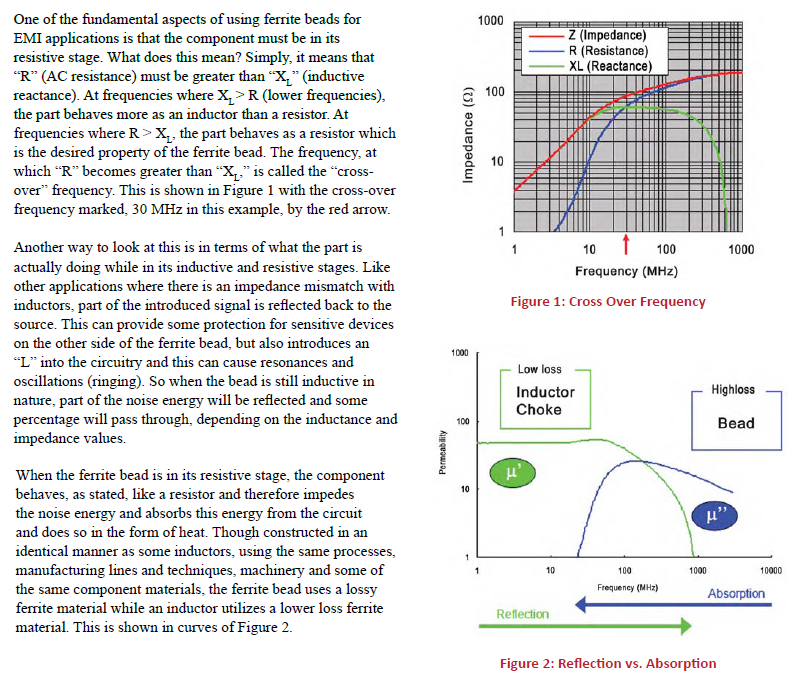
Summary - probably best not to use ferrite beads because they only really start to come into their own above 30 MHz.

Basically I think some of the problems you might be trying to solve are best left in the "inductor" arena whilst maybe the 10MHz sq wave (and more importantly its harmonics) may be dealt with by using ferrite beads.

However, my advise generally is - use ground planes followed by very good capacitor decoupling on all chip power supplies and if you can use small resistors feeding power to vulnerable places (maybe 1 ohm to 10 ohm). If this doesn't prove successful I would want to know why and possibly improve grounding and decoupling before inserting inductors and certainly before considering ferrite beads.

\$\endgroup\$
5
  • \$\begingroup\$ How about 40MHz on-board oscillator and a bunch of TTL signals? My video signal bandwidth is 200MHz. I thought that high frequency components of the TTL square wave signals might compromise the signal. I see why I should use small resistors - low pass. But, isn't that a good practice to have a bead to reduce the possibility of some external high frequency signals entering the power supply line? FB are cheap, and do not seem to harm the circuit. Why do you recommend considering them last? I know about 1-100ohm resistors in TTL lines, would it be a bad idea to place a suitable FB in series ? \$\endgroup\$
    – Nazar
    Commented Jun 12, 2014 at 14:47
  • 1
    \$\begingroup\$ I design data transmission systems that regularly operate at hundreds of Mbits per second. They have to transmit down tens (if not hundreds) of metres of cable and use a mixed bag of cmos, ttl and pecl chips. I'm still to find a use for a ferrite bead in those types of circuit and plenty of others. Never used one and never needed to. Fixed problems by techniques already mentioned and good circuit layout. \$\endgroup\$
    – Andy aka
    Commented Jun 12, 2014 at 16:35
  • \$\begingroup\$ @Naz Maybe it would be interesting to see the good and the great commenting on where they think ferrite beads (as opposed to small inductors) can have a benefit? I'd be interested in reading the answers. \$\endgroup\$
    – Andy aka
    Commented Jun 12, 2014 at 16:41
  • \$\begingroup\$ I know... There are many great talks about FB applications, but I still can not determine which exactly would be useful in my case. However, since the initial question is about the position of the FB within a circuit, most of people do not engage in the conversation. Here's an example page5 for FPGA power filtering. I also saw recommendations to use FB between AVcc and DVcc to power ADCs or DACs. \$\endgroup\$
    – Nazar
    Commented Jun 12, 2014 at 18:26
  • \$\begingroup\$ @Naz On page 5 they are using the FB for PLL supply filtering, not digital switching circuitry. \$\endgroup\$
    – dext0rb
    Commented Jun 12, 2014 at 22:15
2
\$\begingroup\$

Both setups may work. Which is better is governed by capacitor values, their ESLs and the power delivery network downstream.

In the left-hand setup, the PDN should provide low impedance path at lower frequencies. This is the requirement for this setup to work.

The potential advantage of paralleling two capacitors is lower power impedance in a broader range (assuming 0.1 uF and 10 uF cover different frequency ranges). As for the notorious anti-resonance of the two capacitors - look at impedance frequency curves. The situation when it happens is when one capacitor is still capacitor and another one is an inductor. This should not be the case. So, the answer provided by Spehro makes sense as well.

As for the right setup, it may work also. But note that C1 is the only one to provide power when the bead is closed - so its responsibility is huge. The left larger capacitor may not be needed in close proximity (as assumed by the pic I guess). If the bead closes early (say in units of MHz or tens of MHz), then it should provide low impedance path at kHz (or units of MHz) frequencies where location requirements are relaxed (as light wavelength is on the order of tens of meters at these frequencies). But it depends.


Appendix

Below are some general considerations re ferrite beads that might be interesting.

Consider for simplicity the setup with only one capacitor. The main purpose of the second capacitor in the pi setup is to provide low impedance to power at lower frequencies:
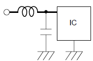
enter image description here

Capacitance value required

Murata's application note, page 11, says

enter image description here

I guess, the way the derived the formula was as follows. They assumed reactance of the inductor and the capacitor equal (Lw=1/cw), calculated frequency, expressed Zt in terms of frequency to get the equation. This is not correct in general. First, impedance of a capacitor in general does not equal to 1/Cw, especially at high frequencies where ESL dominates. Second, the impedance of the capacitor should be much (orders of magnitude) smaller than the impedance of the inductor, not just smaller (2x or 3x times smaller wouldn't work).

The correct way would be to compare the impedance-frequency curves of the capacitor and inductor (accounting for the DC bias used, ideally) and to make sure the impedance of the capacitor is much smaller then the impedance of the inductor where it needs to be. It is not simply some capacitance value needed. The required value of the capacitor's impedance (at some frequency) may be calculated as deltaV/current, where deltaV is an allowable voltage fluctuation and current is the current amplitude at this frequency.

Operation of a ferrite bead

Let's consider as an example this bead BLM03AX241SN1: enter image description here
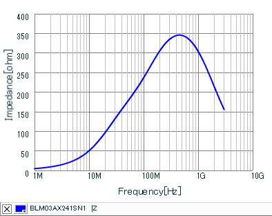
Typical impedance of a power delivery network (PDN) seen in PCB with power/ground planes is from hundreds mOhm to units of Ohms. So the bead is effectively an open connection (resistance ~100 Ohm) starting from several MHz.

It means the whole PDN is cut off from the chip. All hope is for the capacitor. Thus, the importance of the capacitor, if a ferrite bead is used, becomes paramount. Unproperly chosen capacitor would make the chip inoperable. Badly selected bypass cap wouldn't be such a problem if a bead is not used due to action of other capacitors (in parallel).

IR drop at low frequencies

Ferrite beads for power filtering are usually designed as low-q inductors to prevent parasitic resonance. So, DC resistance of ferrite beads is made intentionally high. Often it is about 500 mOhm or even several Ohms. Select a bead with an appropriate DC resistance (there are special series for power lines with relatively low DC resistance). Make sure you can tolerate IR drop given your DC current (say, 10 mA current at 500 mOhm produce 5 mV drop).

High frequencies (>500 MHz)

Inductor is open. Impedance of the capacitor would likely be relatively high (~500 mOhm or even Ohms).

W/o the bead, other capacitors on the board, as well as, planar capacitance of the power planes work for us. And they are all in parallel to the bypass capacitor decreasing PDN impedance. Yes, other capacitors may be located far away, but the planar inductance of the power planes is also very small (current is less concentrated than when flowing in a trace). So, they all have some positive input, despite inductance on the way to them.

This is the reason, ferrite beads are not recommended in high-frequency, high-current circuits (e.g. digital processors), because every hundred mOhm of additional PDN impedance may be critical.

Summary

A ferrite bead may be useful in effectively blocking external noise (or vice versa, noise from the chip) withing some frequency range, while providing a DC connection (to charge the bypass cap). A bead may have substantial DC resistance producing DC voltage drop. A bead increases overall PDN impedance (I guess, at all frequencies), which might be unwelcome at high frequencies, where capacitors stop working well. Choice of the bypass cap becomes paramount. Always use impedance-frequency curves for both capacitor and the inductor (not just plain values of L and C).
\$\endgroup\$
1
  • \$\begingroup\$ I believe Murata's application note is no longer at the given link, but can be found at mouser.com/pdfDocs/c39e.pdf, or by looking for the document named "C39E." \$\endgroup\$
    – addaon
    Commented May 19 at 20:58
1
\$\begingroup\$

I would avoid the right-hand arrangement because it is more likely to result in undesirable resonant behavior (measured at Vout) at some frequencies.

This may be useful.

\$\endgroup\$
3
  • \$\begingroup\$ Can you give some estimates for that in terms of L1, C1, and C2? \$\endgroup\$
    – Samuel
    Commented Jun 11, 2014 at 21:07
  • \$\begingroup\$ You want the Q of the circuit involving the load capacitor, the inductance of the bead (in the region where it is inductive) and the trace resistance to not be too high, so you want Xc to be low compared to trace resistance, cap ESR plus bead resistance. \$\endgroup\$ Commented Jun 11, 2014 at 21:43
  • \$\begingroup\$ @Samuel The values for caps are on the picture (10uF and 0.1uF) as common values for bypass. I have not chosen the ferrite bead, since I do not know which kind is most suitable for filtering power line. I plan to place FBs between every LDO and consumption element (ADC, DAC, OpAmp). If you have a suggestion, please, let me know. \$\endgroup\$
    – Nazar
    Commented Jun 12, 2014 at 13:23
0
\$\begingroup\$

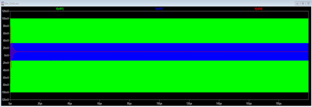
I'm not a filter expert, but the circuit on the right forms a pi type filter. I ran a simulation with LT Spice IV (it's free!) investigating these two configurations for something I'm working on. The circuit on the right works about as well as the circuit on the left from what i can tell. be advised i did not use your exact circuit values. These arrangements attenuate well (red waveform). The green waveform is +/- 100 mV square wave @ 25 MHz. My inductor: 600 ohms at 100 MHz (1.9 uH), caps are .1uF and .01uF. There is slightly better performance when the larger cap is placed closest to the noise source. If you move the ferrite bead so that is closest to the load, it yields the worst performance, but does attenuate (blue waveform).

enter image description here

\$\endgroup\$
0
\$\begingroup\$

If you are engineering a circuit then a ferrite bead should only be used for converting noise energy in the frequency band where the bead is resistive into heat. This is in the 10's to 100's of MHz range.

In DC applications they are good at removing switching artefacts from the outputs of switch mode power supplies. A linear regulator would let noise at those frequencies pass through unattenuated, but putting a ferrite bead between the SMPS output and the linear regulator converts the VHF switching noise to heat. Even for this application a significant amount of simulation (if a realistic model is available for the DC currents the component will be operating at is available) and/or empirical testing is needed, particularly its transient performance.

Ferrite beads are not very suitable for use as a poor-man's inductor in LC filters that have significant DC current flowing through them because they begin to saturate at a small fraction of their rated current and all their characteristics change.

Taking a step back, if a voltage rail is too noisy then its impedance is not low enough at the frequencies current is drawn from it. It is therefore perverse to start by putting a component in the circuit that does the exact opposite of what is needed to reduce the problem, i.e., better designed bulk and/or decoupling capacitance to lower the impedance of the voltage rail at those frequencies.

Putting ferrite beads on the digital supply leads of ICs to "filter" the noise they generate is almost certainly wrong. All that is achieved is compromised performance of the digital part of the IC that has to be mitigated by adding more charge storage capacitors on the IC side of the ferrite bead. A correct solution (along with some others, see below) is better decoupling to lower the supply impedance.

If a small section of sensitive analogue circuitry needs a lower noise supply and only draws mA rather than Amps, then a safer option than an ferrite bead + C is to use an RC filter, possibly with a ferrite bead to filter any very high frequency (>10MHz) noise. The R will damp any tendency of the circuit to ring. Start with the ferrite replaced with a zero-ohm link.

No filter other than well placed and connected decoupling capacitors may be needed if the layout of the circuit is good. E.g., route power to sensitive and noisy circuitry using separate tracks from a single point (i.e., don't tap off power for sensitive circuitry from tracks feeding power to noisy circuitry) and keep noisy circuitry and tracks partitioned from sensitive circuitry and tracks. If possible use a solid ground plane. On 2-layer boards wire links or zero-ohm resistors to cross over tracks might be better than compromising the integrity of the ground plane.

Another way to reduce digital noise it to use series damping/termination resistors or reduce slew rates / drive strength to the minimum required on all digital outputs. If using external resistors for series damping/termination then 33 ohms is a good value to start with for most logic ICs (assuming 50 ohm is the target impedance). If the length of the tracks is long relative to the transition speed of the logic then controlled impedance routing and termination is essential for low noise and reliable performance.

\$\endgroup\$

Your Answer

By clicking “Post Your Answer”, you agree to our terms of service and acknowledge you have read our privacy policy.

Not the answer you're looking for? Browse other questions tagged or ask your own question.