0
\$\begingroup\$

schematic

simulate this circuit – Schematic created using CircuitLab

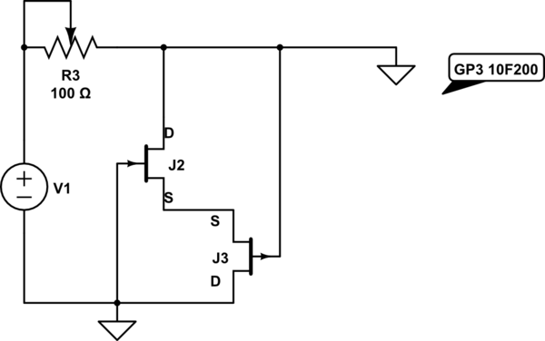
At a coffee house recently, I saw a napkin drawn schematic at the table before the waitress cleaned up after the previous patron. I do not remember the part number for the P ch JFET, but the N CH was MPF102. I cannot figure out what the point of such a circuit would be. It looks to me like the JFETs are going to be biased off unless the voltage rises past the source drain breakdown voltage. Anything that high would damage the microcontroller input pin. What am I missing here?

\$\endgroup\$
5
  • \$\begingroup\$ let's just say, if you were a spy following a person of interest, they just gave you the slip :) \$\endgroup\$ Commented May 7, 2015 at 11:46
  • 3
    \$\begingroup\$ Don't believe everthing you see written on a napkin left lying on a table. \$\endgroup\$ Commented May 7, 2015 at 12:06
  • \$\begingroup\$ I'd GUESS they were aiming a a current source. \$\endgroup\$
    – Russell McMahon
    Commented May 7, 2015 at 16:20
  • 1
    \$\begingroup\$ I found this:lcbsystems.com/LambdaDiode.html \$\endgroup\$
    – steverino
    Commented May 8, 2015 at 18:30
  • \$\begingroup\$ If GP3 is set to wake on change then the goal may have been to wake a sleeping part when the voltage rises. I have used a zener for this before. But this approach (if properly biased, unlike the circuit I copied) would not eat battery until the wakeup like the zener would. It would make sense that someone would use two FETs and a few resistors in preference to a zener and a resistor if battery life is critical. \$\endgroup\$
    – steverino
    Commented May 8, 2015 at 18:48

3 Answers 3

3
\$\begingroup\$

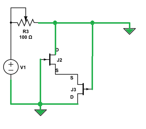
The circuit is wrong/useless. Look at the 0V connections - the series combination of J1 and J2 are shorted by 0V. This effectively makes the circuit V1 in parallel with R3: -

enter image description here

\$\endgroup\$
3
\$\begingroup\$

Ignoring that spurious extra ground at the top right (presumably supposed to go to the microcontroller GPIO), the JFETs will present a low impedance near 0V and increase for (poorly controlled) higher voltages. JFETs are depletion devices (normally 'on').

I don't see much point to this circuit as drawn. Sometimes JFETs are useful as low-leakage clamp diodes, but that's not what's happening here.

\$\endgroup\$
2
\$\begingroup\$

I believe steverinos' comment to the question :

I found this:lcbsystems.com/LambdaDiode.html – steverino May 8 '15 at 18:30

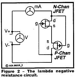
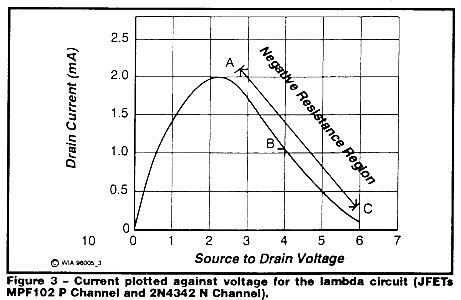
was on the right track. It appears to be a lambda diode arrangement as described in this article:

A Dip Meter Using the Lambda Negative Resistance Circuit by Lloyd Butler VK5BR (Originally published in Amateur Radio, January 1997)

The lambda negative resistance circuit Lambda diode voltage vs current curve

here is an article from 1975 presenting the lambda diode and a couple applicaions.

while researching this a little bit I came across following articles of interest:

Anyway, thought I may share my insights to the question I stumbled upon. Cheers

\$\endgroup\$
2
  • \$\begingroup\$ The ground at the top right ruins this functionality, though. It shorts out both FETs. If you remove it, you are left with a lambda diode, though, yes. \$\endgroup\$
    – Hearth
    Commented Dec 14, 2019 at 20:18
  • \$\begingroup\$ Yea, completely agree, although if we consider that the original source of the schematic was a napkin drawing, I would consider some flexibility to the interpretation and could say that maybe a triangle could be the representation of a port or conection to somewhere else instead of a ground connection. Was nice to have stumbled across the question in any case. \$\endgroup\$ Commented Dec 16, 2019 at 12:45

Your Answer

By clicking “Post Your Answer”, you agree to our terms of service and acknowledge you have read our privacy policy.

Not the answer you're looking for? Browse other questions tagged or ask your own question.