0
\$\begingroup\$

I need to add over 20 kBytes of RAM to the small device built around ATMega8. Moreover I'm interested to research whether I can substitute it with ATtiny2313. The goal is roughly speaking to store some fast arriving data there before serving them out through serial interface...

I thought of 62256 chips, but with them I need 15 address lines and 8 data lines - somewhat more than I can spare with any of these two MCUs. Meanwhile the matter is to find the solution with smallest (cheapest) MCU possible, so I'm not ready to switch to some ATMega16 or 32 which, I think, will do the trick. I also have found serial SRAM from Microchip, but it seems the speed will be not sufficient for me...

So I'm thinking of using two (?) octal latches - but I'm afraid I'm reinventing the wheel and here could be easier solution. That's why I'm here. This is my current idea:

  • I feed the high and low bytes of the address from outputs of two octal latches;
  • I wire 8 pins (say, PB0..PB7) to both latches and to 8 data lines;
  • Now I need two more pins to control latches and another two for WE and OE of the SRAM chip.

And here are my questions:

  • are two latches enough, is it correct I need no latches on data lines?
  • will 74hct373 be a good choice for latches?
  • is it ok to slightly swap address lines for high byte (i.e. instead of order A8, A9, A10, A11, A12, A13, A14 wire them as A8, A9, A11, A10, A14, A13, A12 for example to simplify routing)?
  • perhaps there is another solution (besides larger MCU, latches or serial SRAM) I've missed?
\$\endgroup\$
1

3 Answers 3

2
\$\begingroup\$

Sounds OK. You are correct, don't put a latch on the Data lines as these are bidirectional. As long as you make sure OE is deasserted when you are programming the address, and you your latch enable lines are never asserted when OE is asserted, then you shouldn't have any problems. It will take additional clock cycles to access the memory, but that's the price you pay for saving pins.

It would basically be something like:

  1. Ensure OE and WE are deasserted
  2. Load address 0..7 onto data lines
  3. Latch into the lower address latch
  4. Load address 8..15 onto data lines
  5. Latch into upper address latch
  6. Either load data onto data lines (for write), or set to input (for read)
  7. Perform operation using OE and WE pins.

Swapping the address lines to the SRAM would be fine - it just means stuff will be stored in a weird order inside the SRAM, but as far as the uC is concerned it will be contiguous. For flash this can be an issue as page accesses would no longer be possible, but SRAM like the 62256 doesn't have that issue as it doesn't use paging.

\$\endgroup\$
1
  • \$\begingroup\$ Tom, thank you very much for all your detailed input (in comments also)! I'll be back to vote up when I have such privilege :) \$\endgroup\$
    – Alumashka
    Commented Dec 8, 2015 at 6:18
2
\$\begingroup\$

There are SRAM devices with SPI interfaces. That is a more reliable and simple solution than trying to emulate data and address bus with port IO.

\$\endgroup\$
5
  • \$\begingroup\$ SPI any memory device is a better solution. It'll probably be faster too, since there's far less setup. \$\endgroup\$ Commented Dec 7, 2015 at 22:25
  • \$\begingroup\$ SPI (when used with a chip that has hardware SPI interface, of course) is quite fast- the Microchip devices run at 20MHz clock, use only a few pins and are dirt-cheap. A hardware SPI runs concurrently with other processing so it most likely has very little cost in terms of CPU cycles. \$\endgroup\$ Commented Dec 7, 2015 at 22:31
  • \$\begingroup\$ Plus many of them have address auto-increment, meaning that each additional byte only takes 16 cycles instead of however many it takes to set up the address for a parallel device. \$\endgroup\$ Commented Dec 7, 2015 at 22:34
  • \$\begingroup\$ Won't be faster. An ATMega can only run its SPI up to FCPU/2. So it takes at least 16 clock cycles to read 8 data bits, plus others for configuring the SPI. This is only true for burst reads. If you are doing single accesses, you have another 32 clock cycles to load the 16bit address in each SPI transaction, so that would take ~50 cycles per byte. Using the parallel approach, even with the setup, would take (if done in ASM) ~15 clock cycles. So for burst reads both would be about the same speed, for single byte access, parallel is about 3 times faster! \$\endgroup\$ Commented Dec 8, 2015 at 0:08
  • \$\begingroup\$ Yes, Tom Carpenter properly explained my own calculations which I've done before setting aside the idea with serial SRAM. Though it really looks much, much simpler in sense of routing. Thanks to Ignacio Vazquez-Abrams for valuable hint, also. \$\endgroup\$
    – Alumashka
    Commented Dec 8, 2015 at 6:14
2
\$\begingroup\$

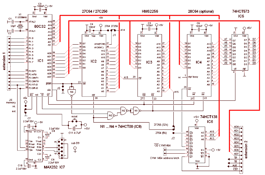
If you are willing to share only 8 of the pins (so you'd need 15 + control lines), you can use a single 74HC573. This was common with the old 8031 circuits since the lower 8 bits of the address was multiplexed with data for external memory access. http://www.dos4ever.com/8031board/schema.gif

\$\endgroup\$

Your Answer

By clicking “Post Your Answer”, you agree to our terms of service and acknowledge you have read our privacy policy.

Not the answer you're looking for? Browse other questions tagged or ask your own question.