2
\$\begingroup\$

I'm studying electrical engineering and we just finished a project where we had to build a power amplifier. But I think I can do better than what we did.

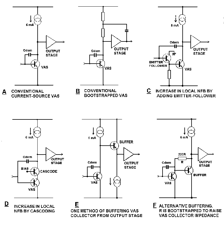
I read Distortion In Power Amplifiers where Douglas Self discusses several VAS stages and their benefits over the basic CEC stage.

VAS stages by Douglas Self

In his results, circuit C and D perform best, apparently by increasing local negative feedback through Cdom.

As I understand it, Cdom is very small (pF) and serves to make the circuit dominantly first order by filtering very high frequencies. Isn't it essentially an open circuit for audio frequencies? The only advantage of C and D seems to be a possibly improved input impedance.

I tried simulating his circuits in LTspice (though all of the biasing circuitry is not included in his schematics), but both the beta-enhanced and cascode don't work very well.

LTspice simulations LTSpice file

Can anyone explain how these circuits work and what I'm doing wrong?

\$\endgroup\$

1 Answer 1

1
\$\begingroup\$

The enhanced VAS does offer high input impedance but its main advantages lie elsewhere. In a standard three stage amplifier the Beta-Enhanced VAS increases the OLG ceiling to something like 115-120dB making more available GNFB for the same closed loop gain, resulting in much lower THD and Zout.

Its main problem is awful clipping behavior. But that can be solved easily with a 220 ohm resistor in series with a clamp diode (normal signal diode like 1N4148) connected from the first transistor's base to the second transistor's collector, giving soft-clipping as well as guaranteed latch free overload characteristics. With that added, the enhanced VAS is a clear winner in all the six configs.

Considering the practical application of the configuration, in your simulation of the enhanced VAS there are a few apparent problems: a)There should be no capacitor in parallel with the emitter resistor of the second transistor. b)The input needs to be in the form of a current (from a collector-output node e.g. the long-tailed pair), referenced to the negative rail. c)The first transistor's collector should be connected to ground, not the positive rail.

\$\endgroup\$

Your Answer

By clicking “Post Your Answer”, you agree to our terms of service and acknowledge you have read our privacy policy.

Not the answer you're looking for? Browse other questions tagged or ask your own question.